TPS51100
TPS51100 is Source DDR Termination Regulator manufactured by Texas Instruments.
Features
- 1 Input Voltage Range: 4.75 V to 5.25 V
- VLDOIN Voltage Range: 1.2 V to 3.6 V
- 3-A Sink/Source Termination Regulator Includes
Droop pensation
- Requires Only 20-μF Ceramic Output Capacitance
- Supports Hi-Z in S3 and Soft-Off in S5
- 1.2-V Input (VLDOIN) Helps Reduce Total Power
Dissipation
- Integrated Divider Tracks 0.5 VDDQSNS for VTT and VTTREF
- Remote Sensing (VTTSNS)
- ±20-m V Accuracy for VTT and VTTREF
- 10-m A Buffered Reference (VTTREF)
- Built-In Soft-Start, UVLO, and OCL
- Thermal Shutdown
- Supports JEDEC Specifications
2 Applications
- DDR, DDR2, DDR3 Memory Termination
- SSTL-2, SSTL-18, and HSTL Termination
3 Description
The TPS51100 is a 3-A, sink/source tracking termination regulator. The device is specifically designed for low-cost and low-external ponent count systems where space is a premium.
The TPS51100 maintains fast transient response, only requiring 20 μF (2 × 10 μF) of ceramic output capacitance. The TPS51100 supports remote sensing functions and all features required to power the DDR and DDR2 VTT bus termination according to the JEDEC specification. The part also supports DDR3 VTT termination with VDDQ at 1.5 V (typical). In addition, the TPS51100 includes integrated sleepstate controls, placing VTT in Hi-Z in S3 (suspend to RAM) and soft-off for VTT and VTTREF in S5 (suspend to disk). The TPS51100 is available in the thermally efficient 10-pin MSOP Power PAD™ package and is specified from
- 40°C to 85°C.
Device Information(1)
PART NUMBER PACKAGE
BODY SIZE (NOM)
HVSSOP (10)
3.00 mm x 3.00 mm
(1) For all available packages, see the orderable addendum at the end of the datasheet.
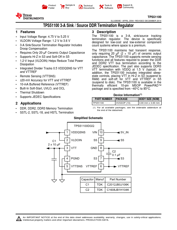
Simplified Schematic
TPS51100DGQ 1 VDDQSNS VIN 10
5V_IN
C1 2 x 10 µF
2 VLDOIN 3 VTT
4 PGND
S5 9 GND 8
S3 7
S5
C2 0.1...