Datasheet4U Logo Datasheet4U.com

TPS22925 - On-Resistance Load Switch

Datasheet Summary

Description

The TPS22925 product family consists of four devices: TPS22925B, TPS22925BN, TPS22925C, and TPS22925CN.

Each device is a 9-mΩ, singlechannel load switch with a controlled slew rate.

channel MOSFET that can operate over an input voltage range of 0.65 V to 3.6 V and ca

Features

  • 1 Input Voltage Range: 0.65 V to 3.6 V.
  • On-Resistance.
  • RON = 9.2 mΩ at VIN = 3.6 V.
  • RON = 9.2 mΩ at VIN = 1.8 V.
  • RON = 10.2 mΩ at VIN = 1 V.
  • RON = 13.1 mΩ at VIN = 0.65 V.
  • 3-A Maximum Continuous Switch Current.
  • Quiescent Current, IQ,VIN = 29 µA at VIN = 3.6 V.
  • Low Control Input Threshold Enables 1.5-, 1.8-, 2.5-, or 3.3-V Logic.
  • Controlled Slew Rate.
  • tR = 97 µs at VIN = 3.6 V (TPS22925Bx).

📥 Download Datasheet

Datasheet preview – TPS22925

Datasheet Details

Part number TPS22925
Manufacturer Texas Instruments
File Size 1.23 MB
Description On-Resistance Load Switch
Datasheet download datasheet TPS22925 Datasheet
Additional preview pages of the TPS22925 datasheet.
Other Datasheets by Texas Instruments

Full PDF Text Transcription

Click to expand full text
Product Folder Sample & Buy Technical Documents Tools & Software Support & Community TPS22925 SLVS840D – NOVEMBER 2015 – REVISED AUGUST 2016 TPS22925 3.6-V, 3-A, 9-mΩ On-Resistance Load Switch 1 Features •1 Input Voltage Range: 0.65 V to 3.6 V • 
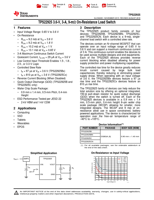
On-Resistance – RON = 9.2 mΩ at VIN = 3.6 V – RON = 9.2 mΩ at VIN = 1.8 V – RON = 10.2 mΩ at VIN = 1 V – RON = 13.1 mΩ at VIN = 0.65 V • 3-A Maximum Continuous Switch Current • Quiescent Current, IQ,VIN = 29 µA at VIN = 3.6 V • Low Control Input Threshold Enables 1.5-, 1.8-, 2.5-, or 3.3-V Logic • Controlled Slew Rate – tR = 97 µs at VIN = 3.6 V (TPS22925Bx) – tR = 810 µs at VIN = 3.6 V (TPS22925Cx) • Reverse Current Blocking (When Disabled) • Quick Output Discharge (QOD) (TPS22925B and TPS22925C only) • Wafer Chip Scale Package: – 0.
Published: |