Datasheet4U Logo Datasheet4U.com

LMK1C1104 - LVCMOS Clock Buffer

Download the LMK1C1104 datasheet PDF (LMK1C1102 included). The manufacturer datasheet provides complete specifications, pinout details, electrical characteristics, and typical applications for lvcmos clock buffer.

Description

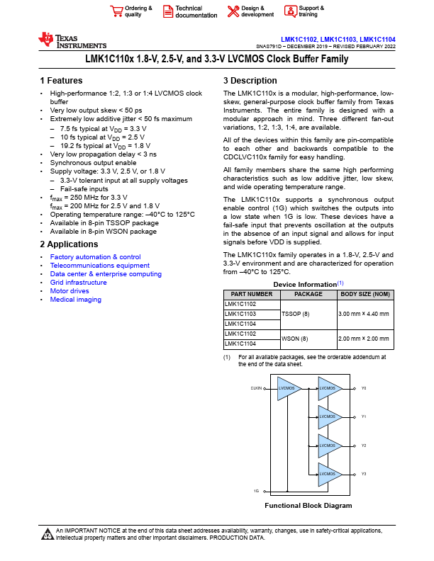
The LMK1C110x is a modular, high-performance, lowskew, general-purpose clock buffer family from Texas Instruments.

The entire family is designed with a modular approach in mind.

Three different fan-out variations, 1:2, 1:3, 1:4, are available.

Features

  • High-performance 1:2, 1:3 or 1:4 LVCMOS clock buffer.
  • Very low output skew < 50 ps.
  • Extremely low additive jitter < 50 fs maximum.
  • 7.5 fs typical at VDD = 3.3 V.
  • 10 fs typical at VDD = 2.5 V.
  • 19.2 fs typical at VDD = 1.8 V.
  • Very low propagation delay < 3 ns.
  • Synchronous output enable.
  • Supply voltage: 3.3 V, 2.5 V, or 1.8 V.
  • 3.3-V tolerant input at all supply voltages.
  • Fail-safe inputs.
  • fm.

📥 Download Datasheet

Note: The manufacturer provides a single datasheet file (LMK1C1102-etcTI.pdf) that lists specifications for multiple related part numbers.
Other Datasheets by Texas Instruments

Full PDF Text Transcription

Click to expand full text
LMK1C1102, LMK1C1103, LMK1C1104 SNAS791D – DECEMBER 2019 – REVISED FEBRUARY 2022 LMK1C110x 1.8-V, 2.5-V, and 3.3-V LVCMOS Clock Buffer Family 1 Features • High-performance 1:2, 1:3 or 1:4 LVCMOS clock buffer • Very low output skew < 50 ps • Extremely low additive jitter < 50 fs maximum – 7.5 fs typical at VDD = 3.3 V – 10 fs typical at VDD = 2.5 V – 19.2 fs typical at VDD = 1.8 V • Very low propagation delay < 3 ns • Synchronous output enable • Supply voltage: 3.3 V, 2.5 V, or 1.8 V – 3.3-V tolerant input at all supply voltages – Fail-safe inputs • fmax = 250 MHz for 3.3 V fmax = 200 MHz for 2.5 V and 1.
Published: |