Click to expand full text
LMK01801
SNAS573D – JANUARY 2012 – REVISED SEPTEMBER 2021
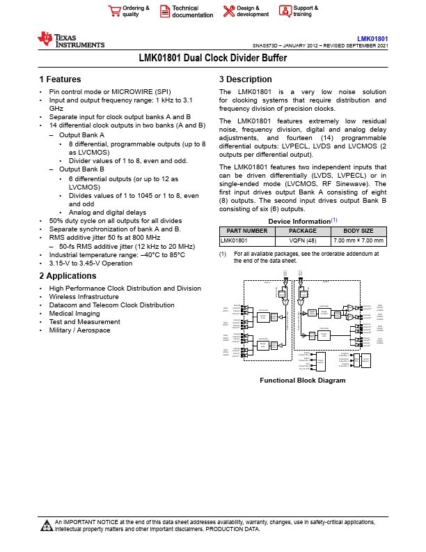
LMK01801 Dual Clock Divider Buffer
1 Features
• Pin control mode or MICROWIRE (SPI) • Input and output frequency range: 1 kHz to 3.1
GHz • Separate input for clock output banks A and B • 14 differential clock outputs in two banks (A and B)
– Output Bank A
• 8 differential, programmable outputs (up to 8 as LVCMOS)
• Divider values of 1 to 8, even and odd. – Output Bank B
• 6 differential outputs (or up to 12 as LVCMOS)
• Divides values of 1 to 1045 or 1 to 8, even and odd
• Analog and digital delays • 50% duty cycle on all outputs for all divides • Separate synchronization of bank A and B. • RMS additive jitter 50 fs at 800 MHz
– 50-fs RMS additive jitter (12 kHz to 20 MHz) • Industrial temperature range: –40°C to 85°C • 3.
 LMK01801 Datasheet