LM98714 Overview
Description
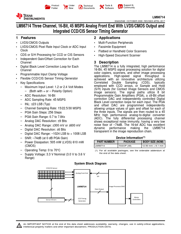
The LM98714 is a fully integrated, high performance 16-Bit, 45 MSPS signal processing solution for digital color copiers, scanners, and other image processing applications. High-speed signal throughput is achieved with an innovative architecture utilizing Correlated Double Sampling (CDS), typically employed with CCD arrays, or Sample and Hold (S/H) inputs (for Contact Image Sensors and CMOS image sensors).
Key Features
- 1 LVDS/CMOS Outputs
- LVDS/CMOS Pixel Rate Input Clock or ADC Input Clock
- CDS or S/H Processing for CCD or CIS Sensors
- Independent Gain/Offset Correction for Each Channel
- Digital Black Level Correction Loop for Each Channel
- Programmable Input Clamp Voltage
- Flexible CCD/CIS Sensor Timing Generator