DS90C402 Overview
Key Specifications
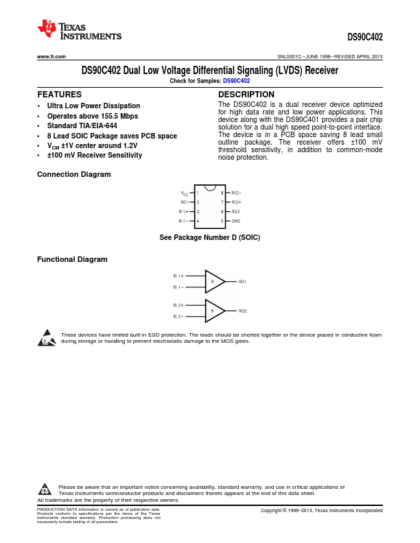
Package: SOIC
Mount Type: Surface Mount
Pins: 8
Operating Voltage: 5 V
Description
The DS90C402 is a dual receiver device optimized for high data rate and low power applications. This device along with the DS90C401 provides a pair chip solution for a dual high speed point-to-point interface.
Key Features
- 2 Ultra Low Power Dissipation
- Operates above 155.5 Mbps
- Standard TIA/EIA-644
- 8 Lead SOIC Package saves PCB space
- VCM ±1V center around 1.2V
- ±100 mV Receiver Sensitivity