CDCVF2505 Overview
Key Specifications
Package: SOIC
Mount Type: Surface Mount
Pins: 8
Operating Voltage: 3.3 V
Description
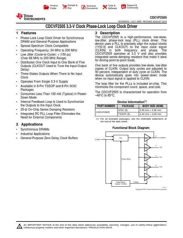
The CDCVF2505 is a high-performance, low-skew, low-jitter, phase-lock loop (PLL) clock driver. This device uses a PLL to precisely align the output clocks (1Y[0-3] and CLKOUT) to the input clock signal (CLKIN) in both frequency and phase.
Key Features
- 1 Phase-Lock Loop Clock Driver for Synchronous DRAM and General-Purpose Applications
- Spread Spectrum Clock Compatible
- Operating Frequency: 24 MHz to 200 MHz
- Low Jitter (Cycle-to-Cycle): < |150 ps| (Over 66 MHz to 200 MHz Range)
- Distributes One Clock Input to One Bank of Five Outputs (CLKOUT Used to Tune the Input-Output Delay)
- Three-States Outputs When There Is No Input Clock
- Operates From Single 3.3-V Supply
- Available in 8-Pin TSSOP and 8-Pin SOIC Packages
- Consumes Less Than 100 mA (Typical) in PowerDown Mode
- Internal Feedback Loop Is Used to Synchronize the Outputs to the Input Clock

