Datasheet4U Logo Datasheet4U.com

CDCVF2505-Q1 - 3.3-V CLOCK PHASE-LOCKED LOOP CLOCK DRIVER

Description

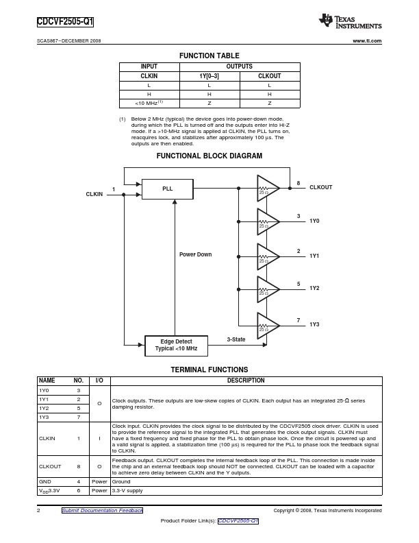
The CDCVF2505 is a high-performance, low-skew, low-jitter, phase-lock loop (PLL) clock driver.

3] and CLKOUT) to the input clock signal (CLKIN).

The CDCVF2505 operates at 3.3 V.

Features

  • 1.
  • Qualified for Automotive.

📥 Download Datasheet

Full PDF Text Transcription

Click to expand full text
CDCVF2505-Q1 www.ti.com........................................................................................................................................................................................... SCAS867 – DECEMBER 2008 3.3-V CLOCK PHASE-LOCKED LOOP CLOCK DRIVER FEATURES 1 • Qualified for Automotive Applications • Phase-Locked Loop Clock Driver for Synchronous DRAM and General-Purpose Applications • Spread-Spectrum Clock Compatible • Operating Frequency: 24 MHz to 200 MHz • Low Jitter (Cycle-to-Cycle): <150 ps Over the Range 66 MHz to 200 MHz • Distributes One Clock Input to One Bank of Five Outputs (CLKOUT Is Used to Tune the Input-Output Delay) • Three-States Outputs When There Is No Input Clock • Operates From Single 3.
Published: |