CDCVF111
description
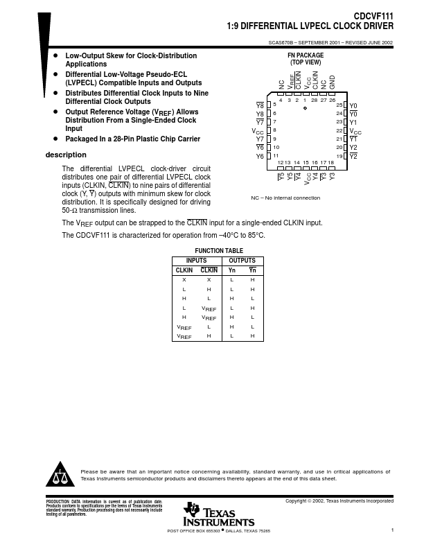
The differential LVPECL clock-driver circuit distributes one pair of differential LVPECL clock inputs (CLKIN, CLKIN) to nine pairs of differential clock (Y, Y) outputs with minimum skew for clock distribution. It is specifically designed for driving 50-Ω transmission lines.
FN PACKAGE (TOP VIEW)
NC VREF CLKIN VCC CLKIN NC GND
Y8 Y8 Y7 VCC Y7 Y6 Y6
4 3 2 1 28 27 26
12 13 14 15 16 17 18
Y0 Y0 Y1 VCC Y1 Y2 Y2
Y5 Y5 Y4 VCC Y4 Y3 Y3
- No internal connection
The VREF output can be strapped to the CLKIN input for a single-ended CLKIN input. The CDCVF111 is characterized for operation from
- 40°C to 85°C.
FUNCTION TABLE
INPUTS
OUTPUTS
CLKIN CLKIN Yn...