CDCUN1208LP
Overview
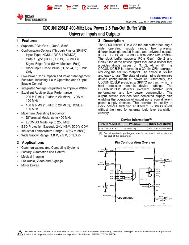
The CDCUN1208LP is a 2:8 fan-out buffer featuring a wide operating supply range, two universal differential/single-ended inputs, and universal outputs (HCSL, LVDS, or LVCMOS) with edge-rate control. The clock buffer supports PCIe Gen1, Gen2 and Gen3.
- 1 Supports PCIe Gen1, Gen2, Gen3
- Configuration Options (Through Pins or SPI/I2C): - Input Type (HCSL, LVDS, LVCMOS) - Output Type (HCSL, LVDS, LVCMOS) - Signal Edge Rate (Slow, Medium, Fast) - Clock Input Divide Value (/1, /2, /4, /8) - IN2 Only
- Low-Power Consumption and Power Management Features, Including 1.8-V Operation and Output Enable Control
- Integrated Voltage Regulators to Improve PSNR
- Excellent Additive Jitter Performance - 200 fs RMS (10 kHz to 20 MHz), LVDS at 100 MHz - 160 fs RMS (10 kHz to 20 MHz), HCSL at 100 MHz
- Maximum Operating Frequency: - Differential Mode: up to 400 MHz - LVCMOS Mode: up to 250 MHz
- ESD Protection Exceeds 2-kV HBM, 500-V CDM
- Industrial Temperature Range (-40°C to 85°C)
- Wide Supply Range (1.8 V, 2.5 V, or 3.3 V)