CDCLVD1216 Description
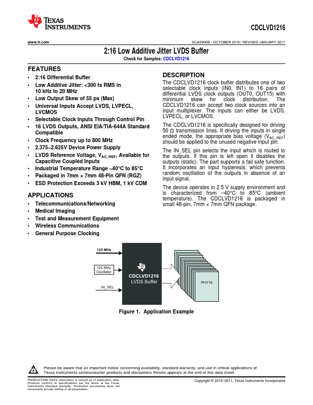
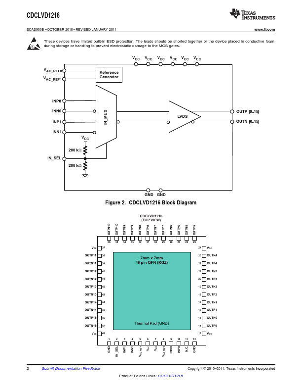
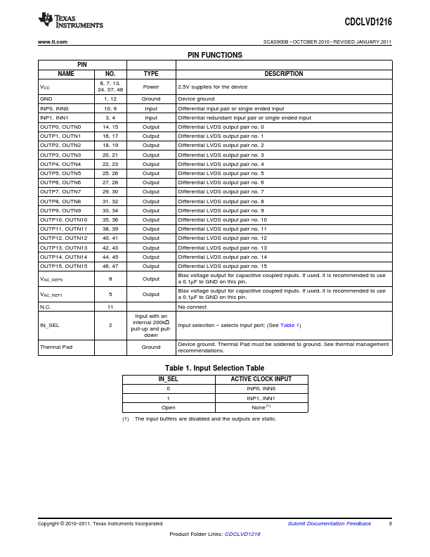
The CDCLVD1216 clock buffer distributes one of two selectable clock inputs (IN0, IN1) to 16 pairs of differential LVDS clock outputs (OUT0, OUT15) with minimum skew for clock distribution. The CDCLVD1216 can accept two clock sources into an input multiplexer. The inputs can either be LVDS, LVPECL, or LVCMOS.
CDCLVD1216 Key Features
- 2:16 Differential Buffer
- Low Output Skew of 55 ps (Max)
- Universal Inputs Accept LVDS, LVPECL
- Selectable Clock Inputs Through Control Pin
- 16 LVDS Outputs, ANSI EIA/TIA-644A Standard
- Clock Frequency up to 800 MHz
- 2.375-2.625V Device Power Supply
- Industrial Temperature Range -40°C to 85°C
- Packaged in 7mm × 7mm 48-Pin QFN (RGZ)
- ESD Protection Exceeds 3 kV HBM, 1 kV CDM