Datasheet4U Logo Datasheet4U.com

CDCLVD1213 - 1:4 Low Additive Jitter LVDS Buffer

Datasheet Summary

Description

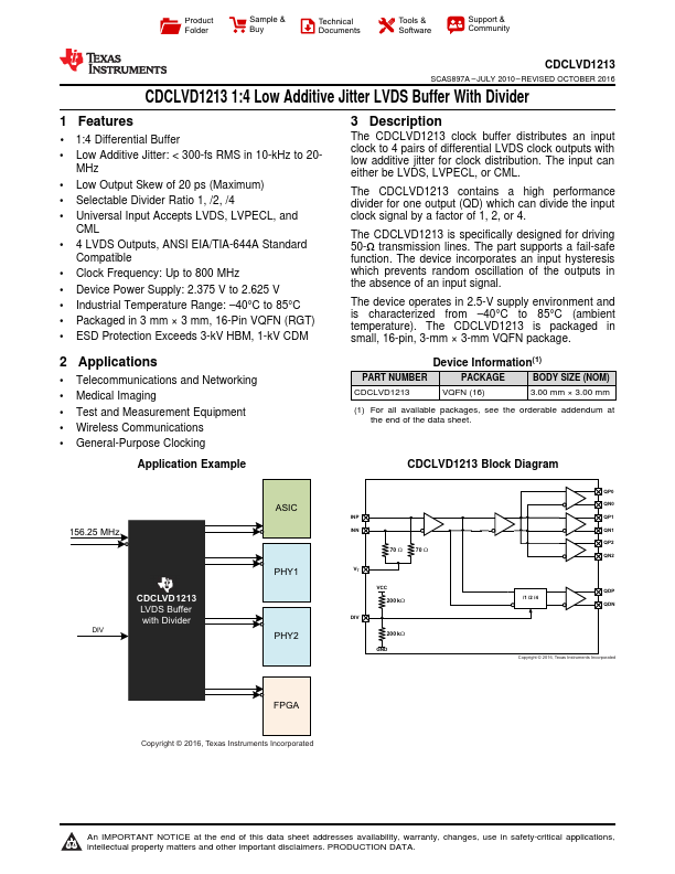
The CDCLVD1213 clock buffer distributes an input clock to 4 pairs of differential LVDS clock outputs with low additive jitter for clock distribution.

The input can either be LVDS, LVPECL, or CML.

Features

  • 1 1:4 Differential Buffer.
  • Low Additive Jitter: < 300-fs RMS in 10-kHz to 20- MHz.
  • Low Output Skew of 20 ps (Maximum).
  • Selectable Divider Ratio 1, /2, /4.
  • Universal Input Accepts LVDS, LVPECL, and CML.
  • 4 LVDS Outputs, ANSI EIA/TIA-644A Standard Compatible.
  • Clock Frequency: Up to 800 MHz.
  • Device Power Supply: 2.375 V to 2.625 V.
  • Industrial Temperature Range:.
  • 40°C to 85°C.
  • Packaged in 3 mm × 3 mm, 16.

📥 Download Datasheet

Datasheet preview – CDCLVD1213

Datasheet Details

Part number CDCLVD1213
Manufacturer Texas Instruments
File Size 874.40 KB
Description 1:4 Low Additive Jitter LVDS Buffer
Datasheet download datasheet CDCLVD1213 Datasheet
Additional preview pages of the CDCLVD1213 datasheet.
Other Datasheets by Texas Instruments

Full PDF Text Transcription

Click to expand full text
Product Folder Sample & Buy Technical Documents Tools & Software Support & Community CDCLVD1213 SCAS897A – JULY 2010 – REVISED OCTOBER 2016 CDCLVD1213 1:4 Low Additive Jitter LVDS Buffer With Divider 1 Features •1 1:4 Differential Buffer • Low Additive Jitter: < 300-fs RMS in 10-kHz to 20- MHz • Low Output Skew of 20 ps (Maximum) • Selectable Divider Ratio 1, /2, /4 • Universal Input Accepts LVDS, LVPECL, and CML • 4 LVDS Outputs, ANSI EIA/TIA-644A Standard Compatible • Clock Frequency: Up to 800 MHz • Device Power Supply: 2.375 V to 2.
Published: |