CDCE18005
Description
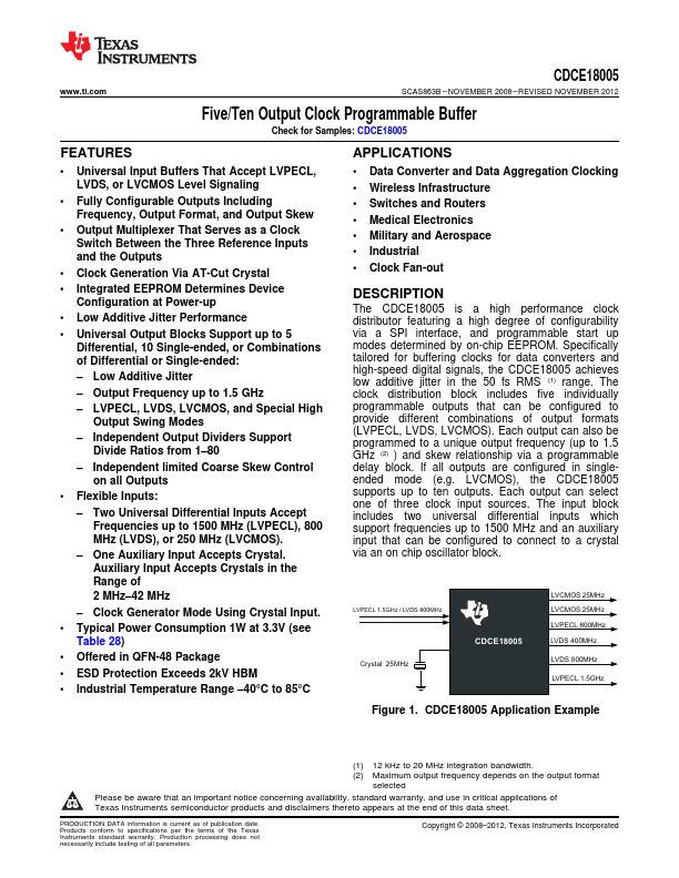
The CDCE18005 is a high performance clock distributor featuring a high degree of configurability via a SPI interface, and programmable start up modes determined by on-chip EEPROM. Specifically tailored for buffering clocks for data converters and high-speed digital signals, the CDCE18005 achieves low additive jitter in the 50 fs RMS (1) range.
Key Features
- Universal Input Buffers That Accept LVPECL, LVDS, or LVCMOS Level Signaling
- Fully Configurable Outputs Including Frequency, Output Format, and Output Skew
- Output Multiplexer That Serves as a Clock Switch Between the Three Reference Inputs and the Outputs
- Clock Generation Via AT-Cut Crystal
- Integrated EEPROM Determines Device Configuration at Power-up
- Low Additive Jitter Performance
- Typical Power Consumption 1W at 3.3V (see Table
- Offered in QFN-48 Package
- ESD Protection Exceeds 2kV HBM
- Industrial Temperature Range –40°C to 85°C