CDC3S04 Overview
Description
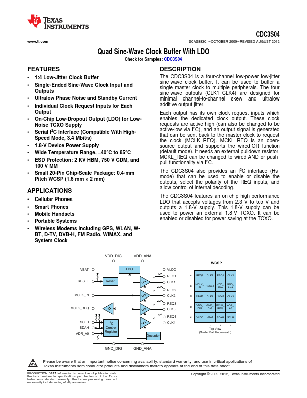
The CDC3S04 is a four-channel low-power low-jitter sine-wave clock buffer. It can be used to buffer a single master clock to multiple peripherals.
Key Features
- 1:4 Low-Jitter Clock Buffer
- Single-Ended Sine-Wave Clock Input and Outputs
- Ultralow Phase Noise and Standby Current
- Individual Clock Request Inputs for Each Output
- On-Chip Low-Dropout Output (LDO) for Low- Noise TCXO Supply
- Serial I2C Interface (Compatible With High- Speed Mode, 3.4 Mbit/s)
- 1.8-V Device Power Supply
- Wide Temperature Range, –40°C to 85°C
- ESD Protection: 2 KV HBM, 750 V CDM, and 100 V MM
- Small 20-Pin Chip-Scale Package: 0.4-mm Pitch WCSP (1.6 mm × 2 mm)