CDC351
CDC351 is 1-Line To 10-Line Clock Driver manufactured by Texas Instruments.
.ti.
CDC351. CDC351I 1-LINE TO 10-LINE CLOCK DRIVER WITH 3-STATE OUTPUTS
SCAS441D
- FEBRUARY 1994
- REVISED OCTOBER 2003
Features
- Low Output Skew, Low Pulse Skew for Clock-Distribution and Clock-Generation Applications
- Operates at 3.3-V VCC
- LVTTL-patible Inputs and Outputs
- Supports Mixed-Mode Signal Operation (5-V Input and Output Voltages With 3.3-V VCC)
- Distributes One Clock Input to Ten Outputs
- Distributed VCC and Ground Pins Reduce Switching Noise
- High-Drive Outputs (- 32-m A IOH, 32-m A IOL)
- State-of-the-Art EPIC-IIB™ Bi CMOS Design
Significantly Reduces Power Dissipation
- Package Options Include Plastic Small-Outline (DW) and Shrink Small-Outline (DB) Packages
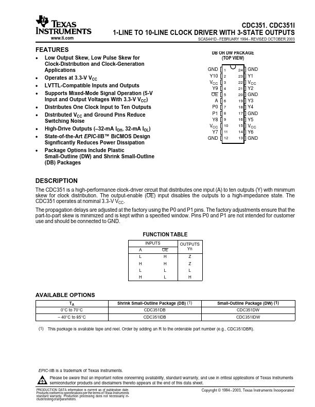
DB OR DW PACKAGE (TOP VIEW)
GND 1 Y10 2 VCC 3
Y9 4 OE 5
A6 P0 7 P1 8 Y8 9 VCC 10 Y7 11 GND 12
24 GND 23 Y1 22 VCC 21 Y2 20 GND 19 Y3 18 Y4 17 GND 16 Y5 15 VCC 14 Y6 13 GND
DESCRIPTION
The CDC351 is a high-performance clock-driver circuit that distributes one input (A) to ten outputs (Y) with minimum skew for clock distribution. The output-enable (OE) input disables the outputs to a high-impedance state. The CDC351 operates at nominal 3.3-V VCC.
The propagation delays are adjusted at the factory using the P0 and P1 pins. The factory adjustments ensure that the part-to-part skew is minimized and is kept within a specified window. Pins P0 and P1 are not intended for customer use and should be connected to GND.
FUNCTION TABLE
INPUTS
OUTPUTS Yn
AVAILABLE OPTIONS
TA 0°C to 70°C
- 40°C to...