CDC2536
CDC2536 is 3.3-V Phase-Lock-Loop Clock Driver manufactured by Texas Instruments.
FEATURES
- Low Output Skew for Clock-Distribution and Clock-Generation Applications
- Operates at 3.3-V VCC
- Distributes One Clock Input to Six Outputs
- One Select Input Configures Three Outputs to
Operate at One-Half or Double the Input Frequency
- No External RC Network Required
- On-Chip Series Damping Resistors
- External Feedback Pin (FBIN) Is Used to
Synchronize the Outputs to the Clock Input
- Application for Synchronous DRAM, High-Speed Microprocessor
- TTL-patible Inputs and Outputs
- Outputs Drive 50-Ω Parallel-Terminated
Transmission Lines
- State-of-the-Art EPIC-IIB™ Bi CMOS Design Significantly Reduces Power Dissipation
- Distributed VCC and Ground Pins Reduce Switching Noise
- Packaged in Plastic 28-Pin Shrink Small-Outline Package
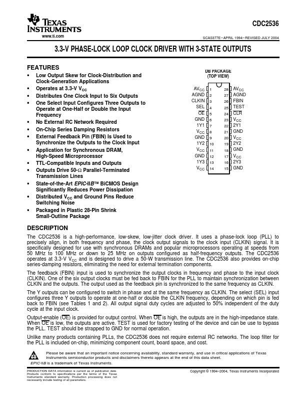
DB PACKAGE (TOP VIEW)
AVCC 1 AGND 2 CLKIN 3
SEL 4 OE 5 GND 6 1Y1 7 VCC 8 GND 9 1Y2 10 VCC 11 GND 12 1Y3 13 VCC 14
28 AVCC 27 AGND 26 FBIN 25 TEST 24 CLR 23 VCC 22 2Y1 21 GND 20 VCC 19 2Y2 18 GND 17 VCC 16 2Y3 15 GND
DESCRIPTION
The CDC2536 is a high-performance, low-skew, low-jitter clock driver. It uses a phase-lock loop (PLL) to precisely align, in both frequency and phase, the clock output signals to the clock input (CLKIN) signal. It is specifically designed for use with synchronous DRAMs and popular microprocessors operating at speeds from 50 MHz to 100 MHz or down to 25 MHz on outputs configured as half-frequency outputs. The CDC2536 operates at 3.3-V VCC and is designed to drive a 50-W transmission line. The CDC2536 also provides on-chip series-damping resistors, eliminating the need for external termination ponents.
The feedback (FBIN) input is used to synchronize the output clocks in frequency and phase to the input clock (CLKIN). One of the six output clocks must be fed back to FBIN for the PLL to maintain synchronization between CLKIN and the outputs. The output used as the feedback pin is synchronized to the same frequency as CLKIN.
The Y outputs can be configured to switch in phase and at the same...