Datasheet4U Logo Datasheet4U.com

CD74HCT365-Q1 - High-Speed CMOS Logic HEX Buffer/Line Driver

Download the CD74HCT365-Q1 datasheet PDF. This datasheet also covers the CD74HC365-Q1 variant, as both devices belong to the same high-speed cmos logic hex buffer/line driver family and are provided as variant models within a single manufacturer datasheet.

Description

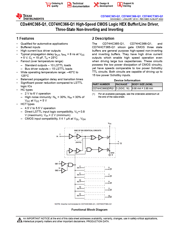
The CD74HC365-Q1, CD74HC366-Q1, and CD74HCT365-Q1 silicon gate CMOS three state buffers are general purpose high-speed non-inverting and inverting buffers.

They have high drive current outputs which enable high speed operation even when driving large bus capacitances.

Features

  • Qualified for automotive.

📥 Download Datasheet

Note: The manufacturer provides a single datasheet file (CD74HC365-Q1-etcTI.pdf) that lists specifications for multiple related part numbers.

Full PDF Text Transcription (Reference)

The following content is an automatically extracted verbatim text from the original manufacturer datasheet and is provided for reference purposes only.

View original datasheet text
CD74HC365-Q1, CD74HC366-Q1, CD74HCT365-Q1 SCHS382A – JANUARY 2010 – REVISED AUGUST 2022 CDx4HC365-Q1, CD74HC366-Q1 High-Speed CMOS Logic HEX Buffer/Line Driver, Three-State Non-Inverting and Inverting 1 Features • Qualified for automotive applications • Buffered inputs • High current bus driver outputs • Typical propagation delay tPLH, tPHL = 8 ns at VCC = 5 V, CL = 15 pF, TA = 25°C • Fanout (over temperature range) – Standard outputs – 10 LSTTL loads – Bus driver outputs – 15 LSTTL loads • Wide operating temperature range: –40°C to 125°C • Balanced propagation delay and transition times • Significant power reduction compared to LSTTL logic ICs • HC types – 2 V to 6 V operation – High noise immunity: NIL = 30%, NIH = 30% of VCC at VCC = 5 V • HCT types – 4.5 V to 5.
Published: |