Datasheet Details
| Part number | CD4050BM |
|---|---|
| Manufacturer | Texas Instruments |
| File Size | 2.31 MB |
| Description | CMOS Hex Inverting Buffer/Converter |
| Datasheet |
 CD4050BM Datasheet CD4050BM Datasheet
|
|
|
Download the CD4050BM datasheet PDF. This datasheet also covers the CD4049UB variant, as both devices belong to the same cmos hex inverting buffer/converter family and are provided as variant models within a single manufacturer datasheet.
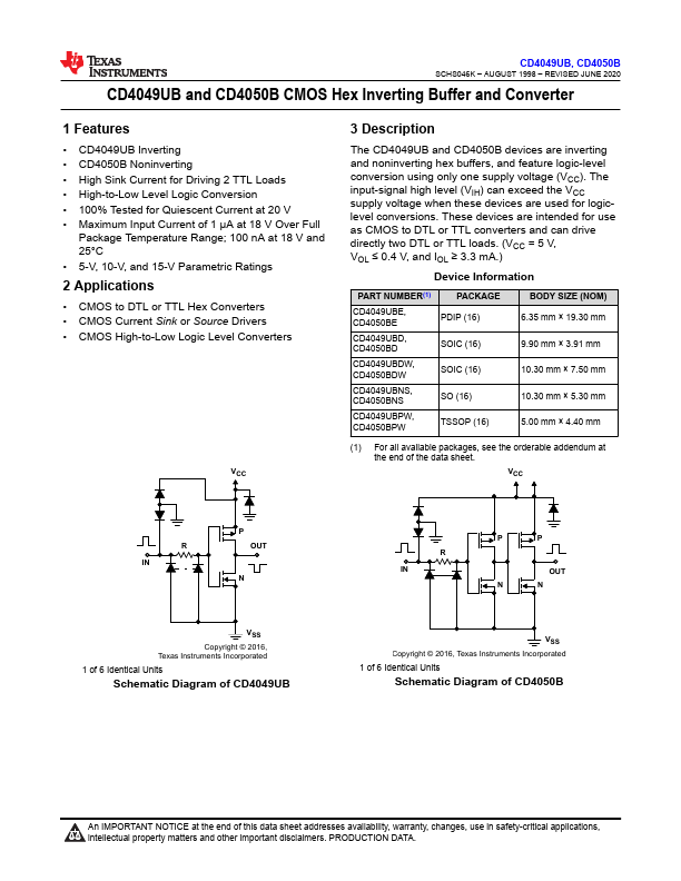
The CD4049UB and CD4050B devices are inverting and noninverting hex buffers, and feature logic-level conversion using only one supply voltage (VCC).
The input-signal high level (VIH) can exceed the VCC supply voltage when these devices are used for logiclevel conversions.
| Part number | CD4050BM |
|---|---|
| Manufacturer | Texas Instruments |
| File Size | 2.31 MB |
| Description | CMOS Hex Inverting Buffer/Converter |
| Datasheet |
CD4050BM Datasheet
|
|
|
|
| Brand Logo | Part Number | Description | Manufacturer |
|---|---|---|---|
| CD4050BM | Hex Inverting/Non-Inverting Buffer | National Semiconductor | |
| CD4050BMS | CMOS Hex Buffer/Converter | Intersil Corporation | |
| CD4050B | CMOS HEX BUFFERS/CONVERTERS | RCA | |
| CD4050B | CMOS Hex Buffer / Converters | Intersil | |
| CD4050B | (CD4049UB / CD4050B) CMOS Hex Buffer/Converters | Harris Corporation |
| Part Number | Description |
|---|---|
| CD4050B | CMOS Hex Inverting Buffer/Converter |
| CD4050BE | CMOS Hex Inverting Buffer/Converter |
| CD4050BF | CMOS Hex Inverting Buffer/Converter |
| CD4050BF3A | CMOS Hex Inverting Buffer/Converter |
| CD4051B | CMOS Single 8-Channel Analog Multiplexer/Demultiplexer |
| CD4051B-Q1 | CMOS Single 8-Channel Analog Multiplexer/Demultiplexer |
| CD4052B | CMOS Single 8-Channel Analog Multiplexer/Demultiplexer |
| CD4053B | CMOS Single 8-Channel Analog Multiplexer/Demultiplexer |
| CD4053B-Q1 | CMOS Single 8-Channel Analog Multiplexer/Demultiplexer |
| CD4001B | CMOS NOR Gates |
Note: Below is a high-fidelity text extraction (approx. 800 characters) for CD4050BM. For precise diagrams, tables, and layout, please refer to the original PDF.
www.ti....