CD4013B
Overview
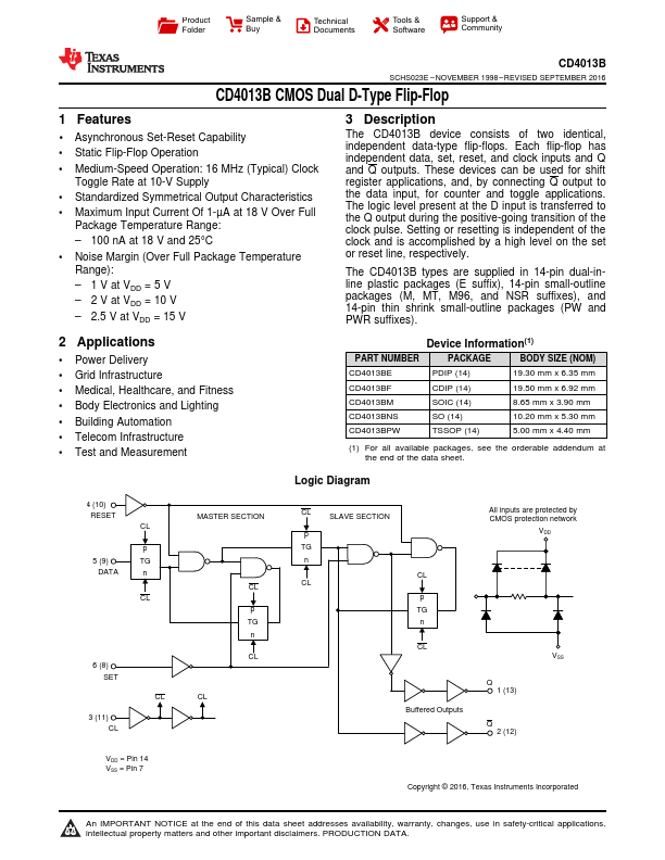
The CD4013B device consists of two identical, independent data-type flip-flops. Each flip-flop has independent data, set, reset, and clock inputs and Q and Q outputs.
- 1 Asynchronous Set-Reset Capability
- Static Flip-Flop Operation
- Medium-Speed Operation: 16 MHz (Typical) Clock Toggle Rate at 10-V Supply
- Standardized Symmetrical Output Characteristics
- Maximum Input Current Of 1-µA at 18 V Over Full Package Temperature Range: - 100 nA at 18 V and 25°C
- Noise Margin (Over Full Package Temperature Range): - 1 V at VDD = 5 V - 2 V at VDD = 10 V - 2.5 V at VDD = 15 V