ADS5263
Overview
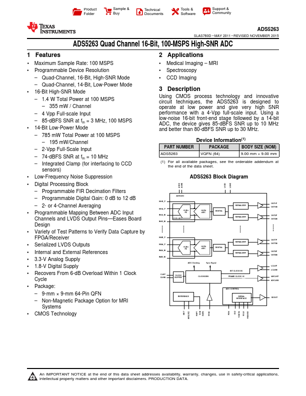
Using CMOS process technology and innovative circuit techniques, the ADS5263 is designed to operate at low power and give very high SNR performance with a 4-Vpp full-scale input. Using a low-noise 16-bit front-end stage followed by a 14-bit ADC, the device gives 85-dBFS SNR up to 10 MHz and better than 80-dBFS SNR up to 30 MHz.
- 1 Maximum Sample Rate: 100 MSPS
- Programmable Device Resolution - Quad-Channel, 16-Bit, High-SNR Mode - Quad-Channel, 14-Bit, Low-Power Mode
- 16-Bit High-SNR Mode - 1.4 W Total Power at 100 MSPS - 355 mW / Channel - 4 Vpp Full-scale Input - 85-dBFS SNR at fin = 3 MHz, 100 MSPS
- 14-Bit Low-Power Mode - 785 mW Total Power at 100 MSPS - 195 mW/Channel - 2-Vpp Full-Scale Input - 74-dBFS SNR at fin = 10 MHz - Integrated Clamp (for interfacing to CCD sensors)
- Low-Frequency Noise Suppression
- Digital Processing Block - Programmable FIR Decimation Filters - Programmable Digital Gain: 0 dB to 12 dB - 2- or 4-Channel Averaging
- Programmable Mapping Between ADC Input Channels and LVDS Output Pins-Eases Board Design
- Variety of Test Patterns to Verify Data Capture by FPGA/Receiver
- Serialized LVDS Outputs
- Internal and External References