The following content is an automatically extracted verbatim text
from the original manufacturer datasheet and is provided for reference purposes only.
View original datasheet text
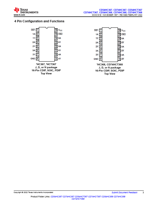
CD54HC367, CD74HC367, CD54HCT367 CD74HCT367, CD54HC368, CD74HC368, CD74HCT368
SCHS181E – NOVEMBER 1997 – REVISED FEBRUARY 2022
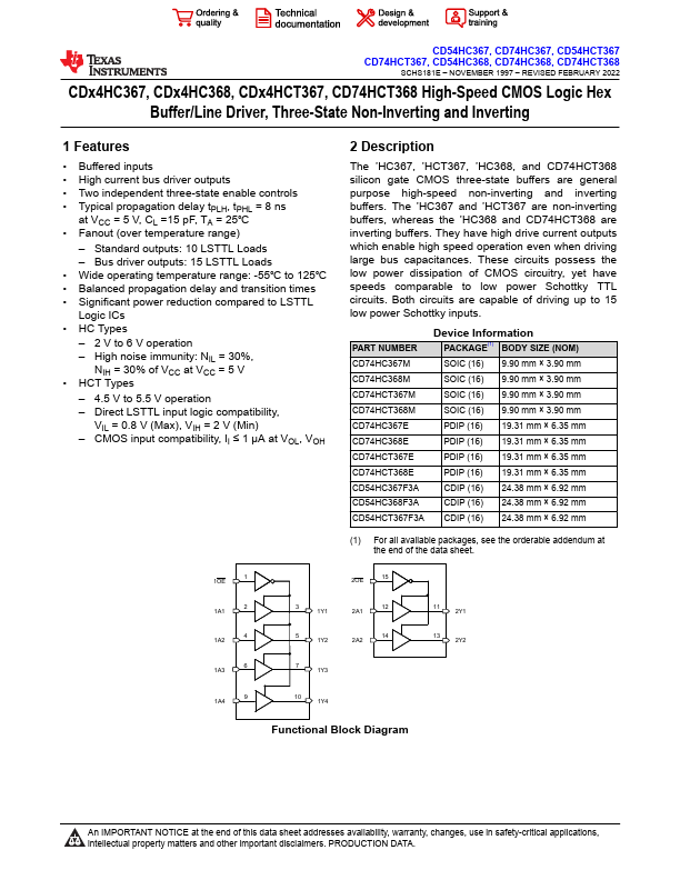
CDx4HC367, CDx4HC368, CDx4HCT367, CD74HCT368 High-Speed CMOS Logic Hex Buffer/Line Driver, Three-State Non-Inverting and Inverting
1 Features
• Buffered inputs • High current bus driver outputs • Two independent three-state enable controls • Typical propagation delay tPLH, tPHL = 8 ns
at VCC = 5 V, CL =15 pF, TA = 25℃ • Fanout (over temperature range)
– Standard outputs: 10 LSTTL Loads – Bus driver outputs: 15 LSTTL Loads • Wide operating temperature range: -55℃ to 125℃ • Balanced propagation delay and transition times • Significant power reduction compared to LSTTL Logic ICs • HC Types – 2 V to 6 V operation – High noise immunity: NIL = 30%,
NIH = 30% of VCC at V
 74HC367 Datasheet