AS1154
AS1154 is Single/Dual LVDS Driver manufactured by austriamicrosystems AG.
Description
The AS1156/AS1154 is a Single/Dual Flow-Through LVDS (Low-Voltage Differential Signaling) Line Driver which accepts and converts LVTTL/LVCMOS input levels into LVDS output signals. The device is perfect for low-power low-noise applications requiring high signaling rates and reduced EMI emissions. The device is guaranteed to transmit data at speeds up to 800Mbps (400MHz) over controlled impedance media of approximately 100Ω. Supported transmission media are PCB traces, backplanes, and cables. The AS1156 is a single LVDS transmitter, and the AS1154 is a dual LVDS transmitter. Outputs conform to the ANSI TIA/EIA-644 LVDS standards. Flow-through pinout simplifies PC board layout and reduces crosstalk by separating the LVTTL/LVCMOS inputs and LVDS outputs. The AS1156/AS1154 operates from a single +3.3V supply and is specified for operation from -40 to +85°C.
2 Key Features
- Flow-Through Pinout Guaranteed 800Mbps Data Rate 250ps Pulse Skew (Max) Conforms to ANSI TIA/EIA-644 LVDS Standards Single +3.3V Supply Operating Temperature Range: -40 to +85°C 8-Pin SOIC Package
- -
- -
- -
3 Applications
Digital Copiers, Laser Printers, Cellular Phone Base Stations, Add/Drop Muxes, Digital Cross-Connects, DSLAMs, Network Switches/Routers, Backplane Interconnect, Clock Distribution puters, Intelligent Instruments, Controllers, Critical Microprocessors and Microcontrollers, Power Monitoring, and Portable/Battery-Powered Equipment.
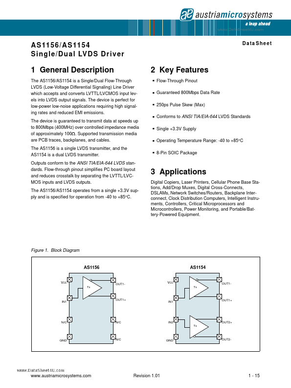
Figure 1. Block Diagram
AS1156
Tx
OUT1-
Tx
OUT1-
IN1
OUT1+
IN1
OUT1+
N/C
N/C
IN2
Tx
OUT2+
N/C
OUT2-
.austriamicrosystems.
Revision 1.01
- 15
AS1156/AS1154
Data Sheet
- P i n o u t
..
4 Pinout
Pin Assignments
Figure 2. AS1156/AS1154 Pin Assignments (Top...