Part number:
SI3473DV
Manufacturer:
Vishay ↗ Siliconix
File Size:
45.79 KB
Description:
P-channel 12-v (d-s) mosfet.
SI3473DV Features
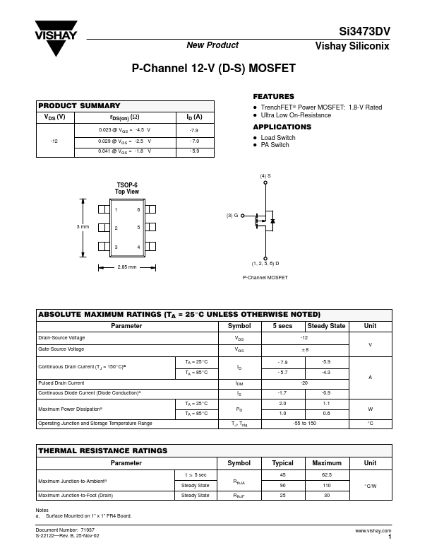
* ID (A) -7.9 - 7.0 - 5.9 D TrenchFETr Power MOSFET: 1.8-V Rated D Ultra Low On-Resistance APPLICATIONS D Load Switch D PA Switch (4) S TSOP-6 Top View 1 6 (3) G 3 mm 2 5 3 4 (1, 2, 5, 6) D P-Channel MOSFET 2.85 mm ABSOLUTE MAXIMUM RATINGS (TA = 25_C UNLESS OTHERWISE NOTED) Parameter Drain-Sou
Datasheet Details
SI3473DV
Vishay ↗ Siliconix
45.79 KB
P-channel 12-v (d-s) mosfet.
📁 Related Datasheet
Si3473DDV P-Channel 12 V (D-S) MOSFET (Vishay)
Si3473 Octal or Quad 2-pair 802.3bt Ethernet Port PoE PSE Controller (Skyworks)
SI3473CDV P-Channel MOSFET (Vishay Siliconix)
Si3471 Autonomous Single Ethernet Port IEEE 802.3bt PoE PSE (Skyworks)
SI3471CDV P-Channel MOSFET (Vishay Siliconix)
Si3472 Octal or Quad 2-pair 802.3bt Ethernet Port PoE PSE Controller (Skyworks)
Si3474 Ethernet Port PoE PSE Controllers (Skyworks)
Si3474 Up to four 802.3bt or eight 802.3at Ethernet Port PoE PSE Controller (Silicon Laboratories)
SI3473DV Distributor