The following content is an automatically extracted verbatim text
from the original manufacturer datasheet and is provided for reference purposes only.
View original datasheet text
www.vishay.com
V40100PGW
Vishay General Semiconductor
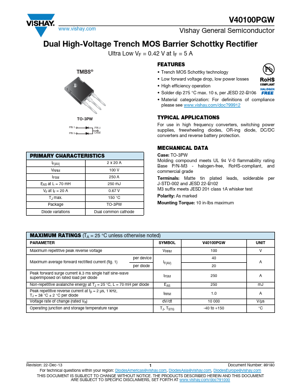
Dual High-Voltage Trench MOS Barrier Schottky Rectifier
Ultra Low VF = 0.42 V at IF = 5 A
TMBS®
FEATURES • Trench MOS Schottky technology • Low forward voltage drop, low power losses • High efficiency operation • Solder dip 275 °C max. 10 s, per JESD 22-B106 • Material categorization: For definitions of compliance
please see www.vishay.com/doc?99912
TO-3PW
PIN 1 PIN 3
PIN 2 CASE
TYPICAL APPLICATIONS
For use in high frequency converters, switching power supplies, freewheeling diodes, OR-ing diode, DC/DC converters and reverse battery protection.
PRIMARY CHARACTERISTICS
IF(AV) VRRM IFSM EAS at L = 70 mH VF at IF = 20 A TJ max. Package
2 x 20 A 100 V 250 A 250 mJ 0.
 V40100PGW Datasheet