• Part: VT98501S1X
  • Description: 3.3V Low Phase Noise Clock Multiplier
  • Manufacturer: Vaishali Semiconductor
  • Size: 77.89 KB
Download VT98501S1X Datasheet PDF
Vaishali Semiconductor
VT98501S1X
VT98501S1X is 3.3V Low Phase Noise Clock Multiplier manufactured by Vaishali Semiconductor.
Description 
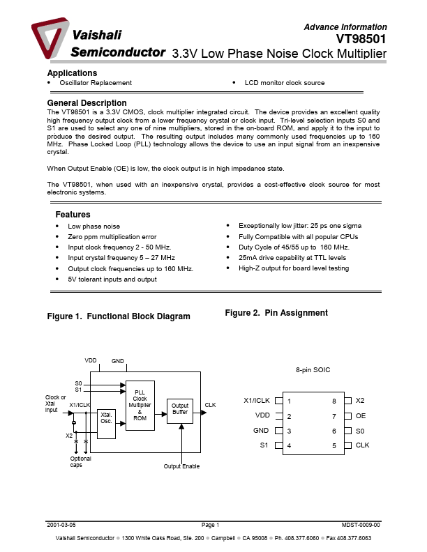
The VT98501 is a 3.3V CMOS, clock multiplier integrated circuit. The device provides an excellent quality high frequency output clock from a lower frequency crystal or clock input. Tri-level selection inputs S0 and S1 are used to select any one of nine multipliers, stored in the on-board ROM, and apply it to the input to produce the desired output. The resulting output includes many monly used frequencies up to 160 MHz. Phase Locked Loop (PLL) technology allows the device to use an input signal from an inexpensive crystal. When Output Enable (OE) is low, the clock output is in high impedance state. The VT98501, when used with an inexpensive crystal, provides a cost-effective clock source for most electronic systems. Features - = - = - = - = - = - = Low phase noise Zero ppm multiplication error Input clock frequency 2 - 50 MHz. Input crystal frequency 5 - 27 MHz Output clock frequencies up to 160 MHz. 5V tolerant inputs and output - = - = - = - = - = Exceptionally low jitter: 25 ps one sigma Fully patible with all popular CPUs Duty Cycle of 45/55 up to 160 MHz. 25m A drive capability at TTL levels High-Z output for board level testing Figure 1. Functional Block Diagram Figure 2. Pin Assignment 8-pin SOIC S0 S1 Clock or Xtal X1/ICLK input PLL Clock Multiplier & ROM Xtal. Osc. Output Buffer X1/ICLK VDD GND S1 1 2 3 4 8 7 6 5 X2 OE S0 CLK X2 Optional caps Output Enable 2001-03-05 Vaishali Semiconductor Page 1 1300 White Oaks Road, Ste. 200 Campbell CA 95008 Ph. 408.377.6060 MDST-0009-00 Fax 408.377.6063 VT98501 Advance Information Table 1. Clock Output Table S1 0 0 0 M M M 1 1 1 S0 0 M 1 0 M 1 0 M 1 CLK 4 x input 5.3125 x input 5 x input 6.25 x input 2 x input 3.125 x input 6 x input 3 x input 8 x input Minimum Input See table 7 20 MHz See table 7 4 MHz See table 7 8 MHz See table 7 See table 7 See table 7 0 = Connect to ground. 1 = Connect directly to VDD M = Leave unconnected...