Datasheet Details
| Part number | CHX2093A |
|---|---|
| Manufacturer | United Monolithic Semiconductors |
| File Size | 76.21 KB |
| Description | 10-30GHz Frequency Multiplier |
| Datasheet |
 CHX2093A Datasheet CHX2093A Datasheet
|
|
|
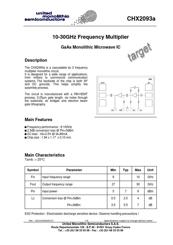
The CHX2093a is a cascadable by 3 frequency multiplier monolithic circuit.
It is designed for a wide range of applications, from military to commercial communication systems.
The backside of the chip is both RF and DC grounds.
| Part number | CHX2093A |
|---|---|
| Manufacturer | United Monolithic Semiconductors |
| File Size | 76.21 KB |
| Description | 10-30GHz Frequency Multiplier |
| Datasheet |
CHX2093A Datasheet
|
|
|
|
| Part Number | Description | Manufacturer |
|---|---|---|
| CHX912 | micro-power Omnipolar Hall effect switch | Cosemitech |
| CHX912L | micro-power Omnipolar Hall effect switch | Cosemitech |
| Part Number | Description |
|---|---|
| CHX2090 | 12-24GHz Frequency Multiplier |
| CHX2090-QDG | Frequency Multiplier |
| CHX2090RBF | 12-24GHz Frequency Multiplier |
| CHX2091 | 20-40GHz Frequency Multiplier |
| CHX2091-99F | Frequency Multiplier |
The following content is an automatically extracted verbatim text from the original manufacturer datasheet and is provided for reference purposes only.