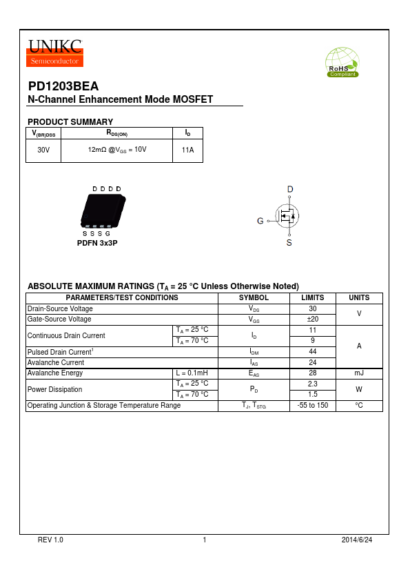
PD1203BEA
N-Channel Enhancement Mode MOSFET
THERMAL RESISTANCE RATINGS
THERMAL RESISTANCE
SYMBOL
TYPICAL MAXIMUM UNITS
Junction-to-Ambient2
RqJA
55 °C / W
1Pulse width limited by maximum junction temperature.
2The value of RqJA is measured with the device mounted on 1in2 FR-4 board with 2oz.Copper , in a still air
environment with TA=25°C。The value in any given application depends on the user's specific board design.
ELECTRICAL CHARACTERISTICS (TJ = 25 °C, Unless Otherwise Noted)
PARAMETER
SYMBOL
TEST CONDITIONS
LIMITS
UNITS
MIN TYP MAX
STATIC
Drain-Source Breakdown Voltage
Gate Threshold Voltage
Gate-Body Leakage
V(BR)DSS
VGS(th)
IGSS
VGS = 0V, ID = 250mA
VDS = VGS, ID = 250mA
VDS = 0V, VGS = ±20V
30
1 1.5
3
V
±100 nA
Zero Gate Voltage Drain Current
On-State Drain Current1
IDSS
ID(ON)
VDS = 24V, VGS = 0V
VDS = 20V, VGS = 0V , TJ = 55 °C
VDS = 5V, VGS = 10V
44
0.03
mA
10
A
Drain-Source On-State
Resistance1
Forward Transconductance1
RDS(ON)
gfs
VGS = 4.5V, ID = 11A
VGS = 10V, ID = 11A
VDS = 5V, ID = 11A
13 17.5 mΩ
9 12
30 S
DYNAMIC
Input Capacitance
Ciss
1040
Output Capacitance
Coss VGS = 0V, VDS = 15V, f = 1MHz
145 pF
Reverse Transfer Capacitance
Gate Resistance
Crss
Rg
VGS = 0V, VDS = 0V, f = 1MHz
104
1.6 Ω
Total Gate Charge2
Gate-Source Charge2
Gate-Drain Charge2
Turn-On Delay Time2
Rise Time2
Turn-Off Delay Time2
Fall Time2
Qg(VGS=10V)
Qg(VGS=4.5V)
Qgs
Qgd
td(on)
tr
td(off)
tf
VDS = 0.5V(BR)DSS,VGS = 10V,
ID = 11A
VDS = 0.5V(BR)DSS,
ID @ 11A, VGS = 10V, RGEN = 6Ω
21
10
nC
3.5
5.2
10
4
nS
20
4
REV 1.0
2 2014/6/24