Datasheet4U.com
🌙
PB210BTF Datasheet | UNIKC
Part:
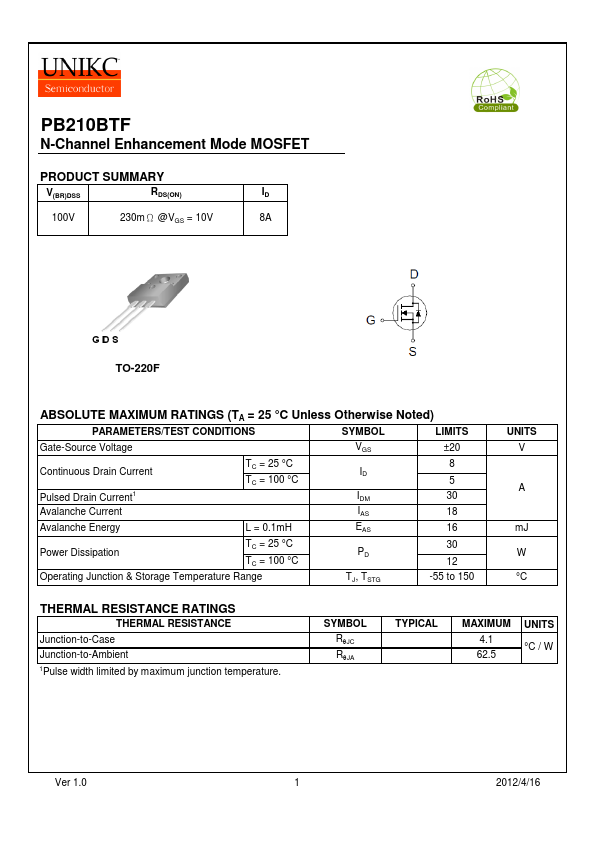
PB210BTF
Description:
N-Channel MOSFET
Category:
MOSFET
Manufacturer:
UNIKC
Size:
348.69 KB
PB210BTF Datasheet (PDF) Download
Related PB210BTF Datasheets
PB210BV MOSFET
PB210BD N-Channel MOSFET
PB210BI MOSFET
PB210BM N-Channel MOSFET
PB210BC N-Channel MOSFET
UNIKC
PB210BTF
×
Close