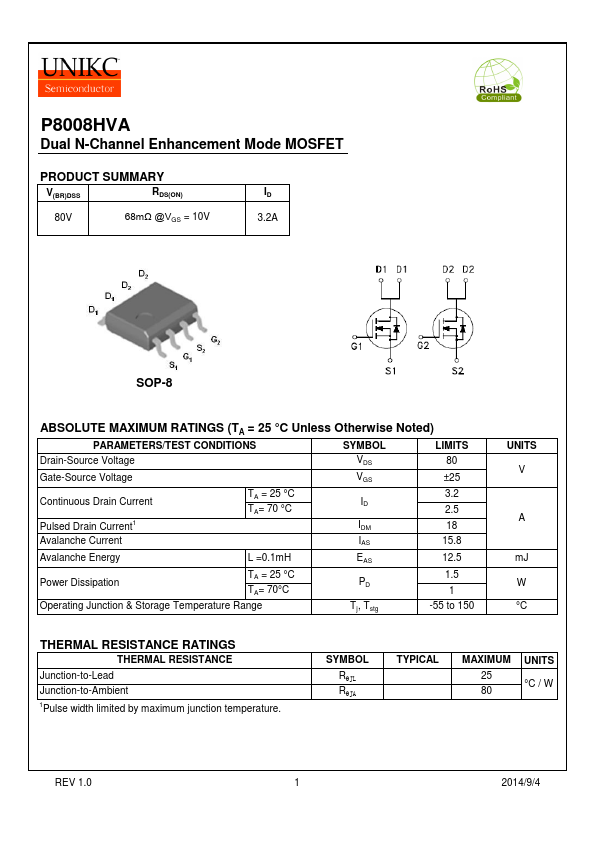
P8008HVA
Dual N-Channel Enhancement Mode MOSFET
ELECTRICAL CHARACTERISTICS (TJ = 25 °C, Unless Otherwise Noted)
PARAMETER
SYMBOL
TEST CONDITIONS
LIMITS
UNITS
MIN TYP MAX
STATIC
Drain-Source Breakdown Voltage
Gate Threshold Voltage
Gate-Body Leakage
V(BR)DSS
VGS(th)
IGSS
Zero Gate Voltage Drain Current
IDSS
VGS = 0V, ID = 250mA
VDS = VGS, ID = 250mA
VDS = 0V, VGS = ±25V
VDS = 64V, VGS = 0V
VDS = 64V, VGS = 0V, TJ = 70 °C
80
1 1.9
3
V
±100 nA
1
mA
10
Drain-Source On-State
Resistance1
RDS(ON)
VGS = 10V, ID = 3A
VGS = 4.5V, ID = 1A
44 68 mΩ
47 78
Forward Transconductance1
gfs
VDS = 10V, ID = 3A
17 S
DYNAMIC
Input Capacitance
Output Capacitance
Reverse Transfer Capacitance
Ciss
Coss
Crss
VGS = 0V, VDS = 25V, f = 1MHz
576
63 pF
42
Gate Resistance
Rg VGS = 0V, VDS = 0V, f = 1MHz
1.2 Ω
Total Gate Charge2
Gate-Source Charge2
Gate-Drain Charge2
Turn-On Delay Time2
Rise Time2
Turn-Off Delay Time2
Fall Time2
Qg
Qgs
Qgd
td(on)
tr
td(off)
tf
VDS = 80V, VGS = 10V,
ID = 3A
VDS = 40V,
ID @ 3A, VGS = 10V, RG = 6Ω
15
2 nC
5
14
6
nS
38
8
SOURCE-DRAIN DIODE RATINGS AND CHARACTERISTICS
Continuous Current
IS
Forward Voltage1
Reverse Recovery Time
VSD IF = 3A, VGS = 0V
trr IF = 3A, dlF/dt = 100A / μS
Reverse Recovery Charge
Qrr
1Pulse test : Pulse Width 300 msec, Duty Cycle 2%.
2Independent of operating temperature.
3Pulse width limited by maximum junction temperature.
1.1 A
1.3 V
30 nS
40 nC
REV 1.0 2 2014/9/4