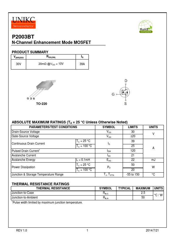
P2003BT Description
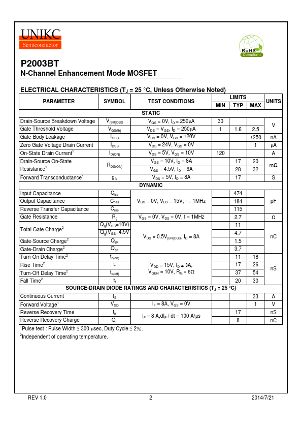
Pulse Width 300 msec, Duty Cycle 2%. 2Independent of operating temperature.
P2003BT is N-Channel MOSFET manufactured by UNIKC.
| Manufacturer | Part Number | Description |
|---|---|---|
| P2003BDG | N-Channel MOSFET | |
| P2003BVG | N-Channel Enhancement Mode Field Effect Transistor | |
| P2003EV8 | P-Channel 30V MOSFET | |
| P2003EVG | P-Channel MOSFET | |
| P2003ND5G | N-/P-Channel FET |
Pulse Width 300 msec, Duty Cycle 2%. 2Independent of operating temperature.