The following content is an automatically extracted verbatim text
from the original manufacturer datasheet and is provided for reference purposes only.
View original datasheet text
P1510ATG
N-Channel Enhancement Mode MOSFET
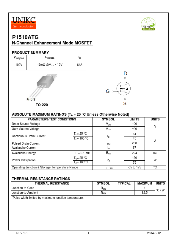
PRODUCT SUMMARY
V(BR)DSS
RDS(ON)
100V
15mΩ @VGS = 10V
ID 64A
TO-220
ABSOLUTE MAXIMUM RATINGS (TA = 25 °C Unless Otherwise Noted)
PARAMETERS/TEST CONDITIONS
SYMBOL
LIMITS
Drain-Source Voltage
VDS 100
Gate-Source Voltage
VGS ±20
Continuous Drain Current Pulsed Drain Current1
TC= 25 °C TC= 100 °C
ID IDM
64 45 200
Avalanche Current
IAS 67
Avalanche Energy
L = 0.1 mH
EAS
224
Power Dissipation
TC= 25 °C TC= 100°C
PD
150 75
Operating Junction & Storage Temperature Range
Tj, Tstg
-55 to 175
UNITS V
A
mJ W °C
THERMAL RESISTANCE RATINGS
THERMAL RESISTANCE Junction-to-Case Junction-to-Ambient 1Pulse width limited by maximum junction temperature.
SYMBOL RqJC RqJA
TYPICAL
MAXIMUM 1
62.5
UNITS °C / W
REV 1.