TGS2303
Overview
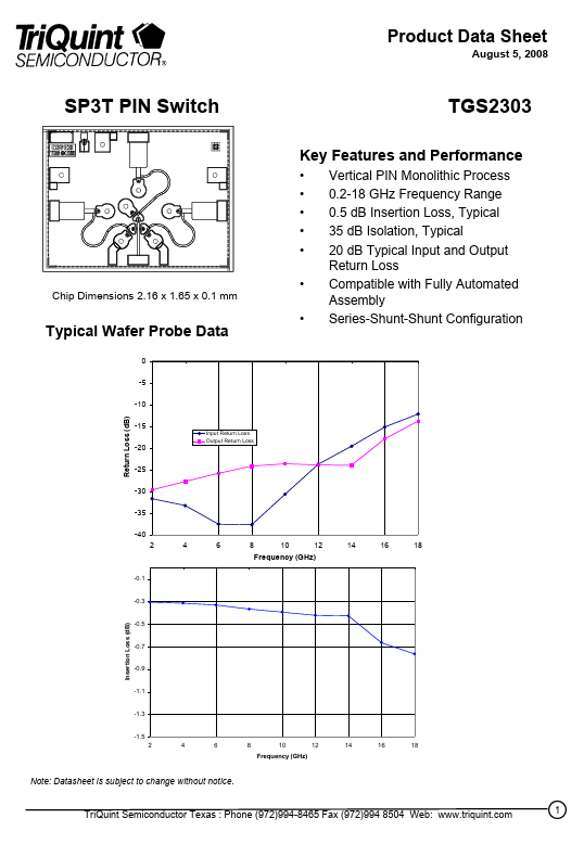
- Vertical PIN Monolithic Process 0.2-18 GHz Frequency Range 0.5 dB Insertion Loss, Typical 35 dB Isolation, Typical 20 dB Typical Input and Output Return Loss Compatible with Fully Automated Assembly Series-Shunt-Shunt Configuration Chip Dimensions 2.16 x 1.65 x 0.1 mm *
- Typical Wafer Probe Data 0 -5 -10 Return Loss (dB) -15 -20 -25 -30 -35 -40 2 4 6 8 10 12 14 16 18 Frequency (GHz) -0.1 -0.3 -0.5 -0.7 -0.9 -1.1 -1.3 -1.5 2 4 6 8 10 Frequency (GHz) 12 14 16 18 Input Return Loss Output Return Loss Note: Datasheet is subject to change without notice. Insertion Loss (dB) TriQuint Semiconductor Texas : Phone (972)994-8465 Fax (972)994 8504 Web: 1 Datasheet pdf - Product Data Sheet TGS2303 Mechanical Drawing Notes:
- GND is the backside of the MMIC
- Please refer to the TGS2304-SCC data sheet for the assembly of the TGS2303-SCC MMIC. The primary difference is the TGS2303 has only 3 output ports. TriQuint Semiconductor Texas : Phone (972)994-8465 Fax (972)994 8504 Web: 2 Datasheet pdf - Product Data Sheet TGS2303 Assembly Process Notes Reflow process assembly notes: * * * *
- Use AuSn (80/20) solder with limited exposure to temperatures at or above 300§C (30 seconds max). An alloy station or conveyor furnace with reducing atmosphere should be used. No fluxes should be utilized. Coefficient of thermal expansion matching is critical for long-term reliability. Devices must be stored in a dry nitrogen atmosphere. Component placement and adhesive attachment assembly notes: * * * * * *
- Vacuum pencils and/or vacuum collets are the preferred method of pick up. Air bridges must be avoided during placement. The force impact is critical during auto placement. Organic attachment can be used in low-power app