TGA2902-SCC-SG
Overview
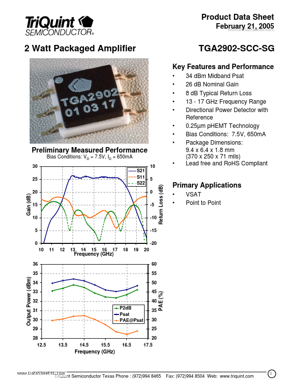
- Gain (dB)
| Part | TGA2902-SCC-SG |
|---|---|
| Description | 2 Watt Packaged Amplifier |
| Manufacturer | TriQuint Semiconductor |
| Size | 156.99 KB |
| Part Number | Manufacturer | Description |
|---|---|---|
| CS3817 | Semico | 2x15W filter-free low EMI stereo Class D audio power amplifier |
| LTK5112 | ChipSourceTek | Mono power audio amplifier |
| 4558D | New Japan Radio | DUAL OPERATIONAL AMPLIFIER |