TPCP8003-H
Key Features
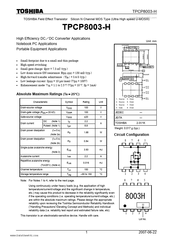
- Small footprint due to a small and thin package High speed switching Small gate charge: QSW = 7.5 nC (typ.) Low drain-source ON-resistance: RDS (ON) = 130 mΩ (typ.) High forward transfer admittance: |Yfs| = 5.4 S (typ.) Low leakage current: IDSS = 10 μA (max) (VDS = 100V) Enhancement mode: Vth = 1.1 to 2.3 V (VDS = 10 V, ID = 1mA)
- 80 V, VGS = 10 V, ID = 2.2 A Symbol IGSS IDSS V (BR) DSS V (BR) DSX Vth RDS (ON) |Yfs| Ciss Crss Coss tr VGS ton 10 V 0V 4.7 Ω VDS = 10 V, VGS = 0 V, f = 1 MHz Test Condition VGS = ±16 V, VDS = 0 V VDS = 100 V, VGS = 0 V ID = 10 mA, VGS = 0 V ID = 10 mA, VGS = -20 V VDS = 10 V, ID = 1 mA VGS = 4.5 V, ID = 1.1 A VGS = 10 V, ID = 1.1 A VDS = 10 V, ID = 1.1 A Min ⎯ ⎯ 100 60 1.1 ⎯ ⎯ 2.7 ⎯ ⎯ ⎯ ⎯ ID