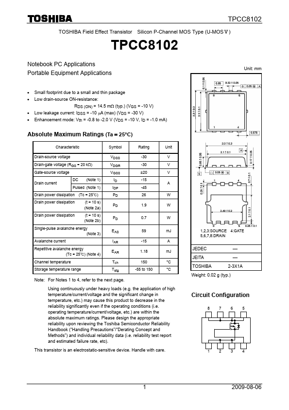
TPCC8102
TPCC8102 is Field Effect Transistor Silicon P-Channel MOS Type manufactured by Toshiba.
TOSHIBA Field Effect Transistor Silicon P-Channel MOS Type (U-MOSⅤ)
Notebook PC Applications Portable Equipment Applications
- -
- - Small footprint due to a small and thin package Low drain-source ON-resistance: RDS (ON) = 14.5 mΩ (typ.) (VGS = -10 V) Low leakage current: IDSS = -10 μA (max) (VDS = -30 V) Enhancement mode: Vth = -0.8 to -2.0 V (VDS = -10 V, ID = -1.0 m A) Unit: mm
Absolute Maximum Ratings (Ta = 25°C)
Characteristic Drain-source voltage Drain-gate voltage (RGS = 20 kΩ) Gate-source voltage Drain current DC (Note 1) Symbol VDSS VDGR VGSS ID IDP PD PD PD EAS IAR EAR Tch Tstg Rating -30 -30 ±20 -15 -45 26 1.9
.Data Sheet.net/
Unit V V V A W W W m J A m J °C °C 1,2,3:SOURCE 5,6,7,8:DRAIN 4:GATE
Pulsed (Note 1) (Tc = 25℃) (t = 10 s) (Note 2a) (t = 10 s) (Note 2b)
Drain power dissipation Drain power dissipation Drain power dissipation
0.7 59 -15 1.18 150 -55 to 150
Single-pulse avalanche energy (Note 3) Avalanche current Repetitive avalanche energy (Tc = 25℃) (Note 4) Channel temperature Storage temperature range
JEDEC JEITA TOSHIBA
⎯ ⎯ 2-3X1A
Weight: 0.02 g (typ.) Note: For Notes 1 to 4, refer to the next page. Using continuously under heavy loads (e.g. the application of high temperature/current/voltage and the significant change in temperature, etc.) may cause this product to decrease in the reliability significantly even if the operating conditions (i.e. operating temperature/current/voltage, etc.) are within the absolute maximum ratings. Please design the appropriate reliability upon reviewing the Toshiba Semiconductor Reliability Handbook (“Handling Precautions”/“Derating Concept and Methods”) and individual reliability data (i.e. reliability test report and estimated failure rate, etc). This transistor is an electrostatic-sensitive device. Handle with care.
Circuit Configuration
8 7 6 5
2009-08-06
Datasheet pdf
- http://..co.kr/
Thermal Characteristics
Characteristic Thermal resistance, channel to...