Datasheet4U Logo Datasheet4U.com

TC7WPN3125FK - Low Voltage/Low Power 2-Bit Dual Supply Bus Buffer

Download the TC7WPN3125FK datasheet PDF (TC7WPN3125FC included). The manufacturer datasheet provides complete specifications, pinout details, electrical characteristics, and typical applications for low voltage/low power 2-bit dual supply bus buffer.

Features

  • Weight: SSOP8-P-0.50A : 0.01 g (typ. ) CSON8-P-0.4 : 0.002 g (typ. ).
  • Level converter for interfacing 1.2-V to 1.8-V, 1.2-V to 2.5-V, 1.2-V to 3.3-V, 1.5-V to 2.5-V, 1.5-V to 3.3-V, 1.8-V to 2.5-V, 1.8-V to 3.3-V or 2.5 V to 3.3-V system.
  • High-speed operation : tpd = 13.7 ns (max) (VCCA = 2.5 ± 0.2 V, VCCB = 3.3 ± 0.3 V) tpd = 14.8 ns (max) (VCCA = 1.8 ± 0.15 V, VCCB = 3.3 ± 0.3 V) tpd = 16.0 ns (max) (VCCA = 1.5 ± 0.1 V, VCCB = 3.3 ± 0.3 V) tpd = 29 ns (max) (VCCA = 1.2 ± 0.1.

📥 Download Datasheet

Note: The manufacturer provides a single datasheet file (TC7WPN3125FC_ToshibaSemiconductor.pdf) that lists specifications for multiple related part numbers.
Other Datasheets by Toshiba Semiconductor

Full PDF Text Transcription

Click to expand full text
TC7WPN3125FK/FC TOSHIBA Digital Integrated Circuit Silicon Monolithic 
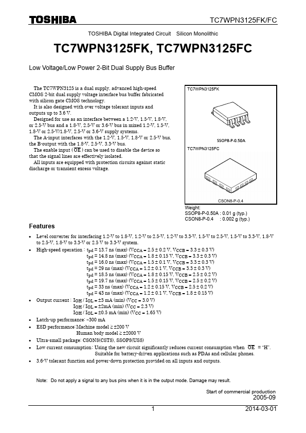
TC7WPN3125FK, TC7WPN3125FC Low Voltage/Low Power 2-Bit Dual Supply Bus Buffer The TC7WPN3125 is a dual supply, advanced high-speed CMOS 2-bit dual supply voltage interface bus buffer fabricated with silicon gate CMOS technology. It is also designed with over voltage tolerant inputs and outputs up to 3.6 V. Designed for use as an interface between a 1.2-V, 1.5-V, 1.8-V, or 2.5-V bus and a 1.8-V, 2.5-V or 3.6-V bus in mixed 1.2-V, 1.5-V, 1.8-V or 2.5-V/1.8-V, 2.5-V or 3.6-V supply systems. The A-input interfaces with the 1.2-V, 1.5-V, 1.8-V or 2.5-V bus, the B-output with the 1.8-V, 2.5-V, 3.3-V bus. 
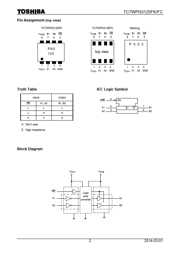
The enable input ( OE ) can be used to disable the device so that the signal lines are effectively isolated.
Published: |