TC7WP3125FC Overview
Key Specifications
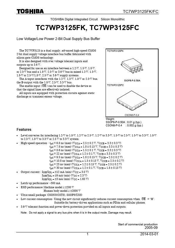
Mount Type: Surface Mount
Pins: 8
Operating Voltage: 1.2 V
Max Voltage (typical range): 2.7 V
Key Features
- Output current : IOH/IOL = ±12 mA (min) (VCC = 3.0 V) IOH/IOL = ±9 mA (min) (VCC = 2.3 V) IOH/IOL = ±3 mA (min) (VCC = 1.65 V)
- Latch-up performance: -300 mA
- ESD performance: Machine model ≥ ±200 V Human body model ≥ ±2000 V
- Ultra-small package: CSON8(CST8), SSOP8(US8)
- Low current co