Datasheet4U Logo Datasheet4U.com

TC7WBD125FK - Dual Bus Switch

Features

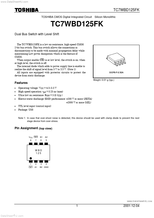
  • Operating voltage: VCC = 4.5~5.5 V High speed operation: tpd = 0.25 ns (max) Ultra-low on resistance: RON = 5 Ω (typ. ) Electro-static discharge (ESD) performance: ±200 V or more (JEITA) ±2000 V or more (MIL) TTL level input (control input) Package: US8 Note 1: In case that over-shoot noise is detected, this device should be used with clamp diode to prevent the next stage device from over-stress. Pin Assignment (top view) VCC OE2 8 7 B.

📥 Download Datasheet

Datasheet preview – TC7WBD125FK

Datasheet Details

Part number TC7WBD125FK
Manufacturer Toshiba Semiconductor
File Size 258.65 KB
Description Dual Bus Switch
Datasheet download datasheet TC7WBD125FK Datasheet
Additional preview pages of the TC7WBD125FK datasheet.
Other Datasheets by Toshiba Semiconductor

Full PDF Text Transcription

Click to expand full text
www.DataSheet4U.com TC7WBD125FK TOSHIBA CMOS Digital Integrated Circuit Silicon Monolithic TC7WBD125FK Dual Bus Switch with Level Shift The TC7WBD125FK is a low on-resistance, high-speed CMOS 2-bit bus switch. This bus switch allows the connections or disconnections to be made with minimal propagation delay while maintaining Low power dissipation which is the feature of CMOS. When output enable (OE) is at low level, the switch is on; when at high level, the switch is off. The internal diode which adds to power supply line is enable to realize the shift of signal level from 5 V to 3.3 V. (Note 1) All inputs are equipped with protector circuits to protect the device from static discharge. Weight: 0.01 g (typ.) Features • • • • • • Operating voltage: VCC = 4.5~5.
Published: |