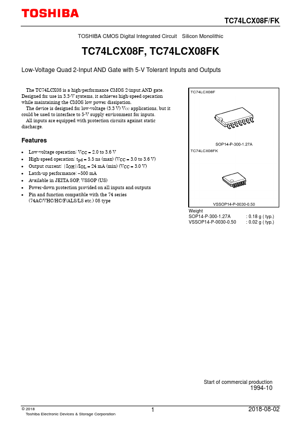
Datasheet4U Logo Datasheet4U.com

TC74LCX08FK - Low-Voltage Quad 2-Input AND Gate

This page provides the datasheet information for the TC74LCX08FK, a member of the TC74LCX08F Low-Voltage Quad 2-Input AND Gate family.

Features

  • Low-voltage operation: VCC = 2.0 to 3.6 V.
  • High-speed operation: tpd = 5.5 ns (max) (VCC = 3.0 to 3.6 V).
  • Output current: |IOH|/IOL = 24 mA (min) (VCC = 3.0 V).
  • Latch-up performance:.
  • 500 mA.
  • Available in JEITA SOP, VSSOP (US).
  • Power-down protection provided on all inputs and outputs.
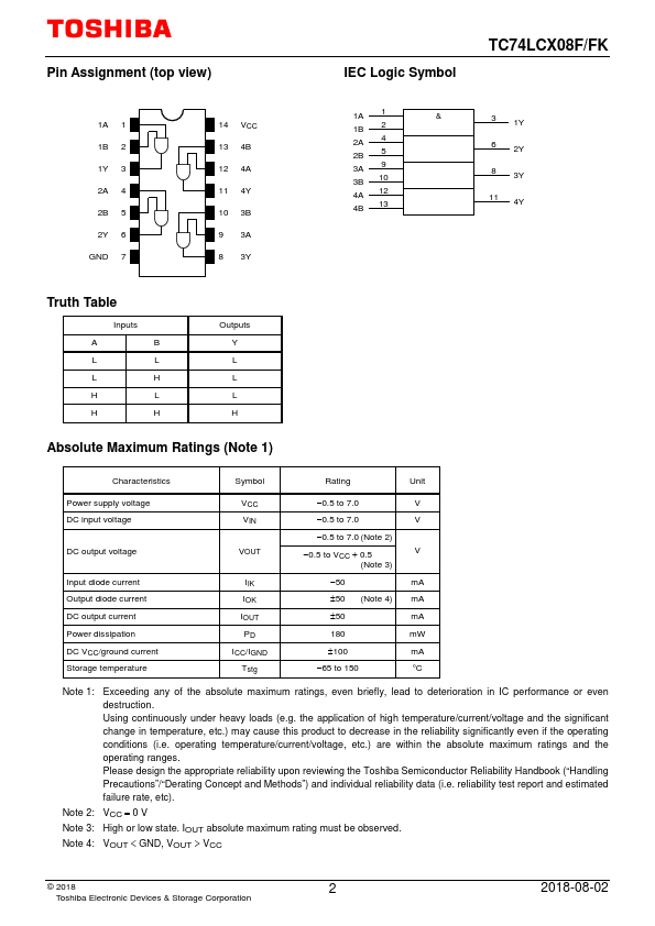
  • Pin and function compatible with the 74 series (74AC/VHC/HC/F/ALS/LS etc. ) 08 type TC74LCX08F TC74LCX08FK Weight SOP14-P-300-1.27A VSSOP14-P.

📥 Download Datasheet

Datasheet preview – TC74LCX08FK
Other Datasheets by Toshiba Semiconductor

Full PDF Text Transcription

Click to expand full text
TC74LCX08F/FK TOSHIBA CMOS Digital Integrated Circuit Silicon Monolithic TC74LCX08F, TC74LCX08FK Low-Voltage Quad 2-Input AND Gate with 5-V Tolerant Inputs and Outputs The TC74LCX08 is a high-performance CMOS 2-input AND gate. Designed for use in 3.3-V systems, it achieves high-speed operation while maintaining the CMOS low power dissipation. The device is designed for low-voltage (3.3 V) VCC applications, but it could be used to interface to 5-V supply environment for inputs. All inputs are equipped with protection circuits against static discharge. Features • Low-voltage operation: VCC = 2.0 to 3.6 V • High-speed operation: tpd = 5.5 ns (max) (VCC = 3.0 to 3.6 V) • Output current: |IOH|/IOL = 24 mA (min) (VCC = 3.
Published: |