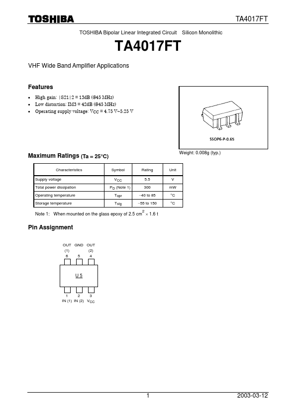
TA4017FT
TA4017FT is TOSHIBA Bipolar Linear Integrated Circuit Silicon Monolithic manufactured by Toshiba.
Features
- -
- High gain: |S21|2 = 13d B (@45 MHz) Low distortion: IM3 = 42d B (@45 MHz) Operating supply voltage: VCC = 4.75 V~5.25 V
Maximum Ratings (Ta = 25°C)
Characteristics Supply voltage Total power dissipation Operating temperature Storage temperature Symbol VCC PD (Note 1) Topr Tstg Rating 5.5 300 -40 to 85 -55 to 150 2 Unit V m W °C °C
Weight: 0.008g (typ.)
Note 1: When mounted on the glass epoxy of 2.5 cm ´ 1.6 t
Pin Assignment
OUT GND OUT (1) (2) 6 5 4
U5
1 2 3 IN (1) IN (2) VCC
2003-03-12
Electrical Characteristics (Ta = 25°C, VCC = 5 V, Zg = Zl = 50 W)
Characteristics Circuit current Band width Input return loss Insertion gain Isolation Output return loss Noise figure Output power at 1d B gain pression Symbol ICC BW |S11|
Test Circuit
Test Condition Non Carrier (Note 2) f = 45 MHz f = 45 MHz f = 400 MHz f = 45 MHz
Min 15 0.7 ¾ 10 ¾ ¾ ¾ ¾ ¾ 0 ¾ 34 ¾
Typ. 19 1 -0.8 13 12.5 -40 -3.5 3 3 2 2 42 42
Max 25 ¾ ¾ 16 ¾ ¾ ¾ 4.5 ¾ ¾ ¾ ¾
Unit m A GHz d B d B d B d B d B
|S21|2 |S12|2 |S22| NF
Fig1 f = 45 MHz f = 45 MHz f = 400 MHz f = 45 MHz f = 400 MHz f1 = 45 MHz, f2 = 44 MHz, Pin = -20d Bm W f1 = 400 MHz, f2 = 399 MHz, Pin = -20d Bm W
Po1d B d Bm W
3 rd order inter modulation
IM3 d B ¾
Note 2: BW is the frequency of 3d B down from |S21| at 45 MHz. CAUTION: This device electrostatic sensitivity. Please handle with caution.
2003-03-12
1000 p F 1 1000 p F 2 33 W IN2 GND 5 IN1 OUT1 6
1000 p F
OUT2
4 1 k W 1 k W
100 p F
1000 p F
10000 p...