SSM3K105TU
SSM3K105TU is Silicon N Channel MOS Type High Speed Switching Applications manufactured by Toshiba.
..
TOSHIBA Field Effect Transistor Silicon N Channel MOS Type
High Speed Switching Applications
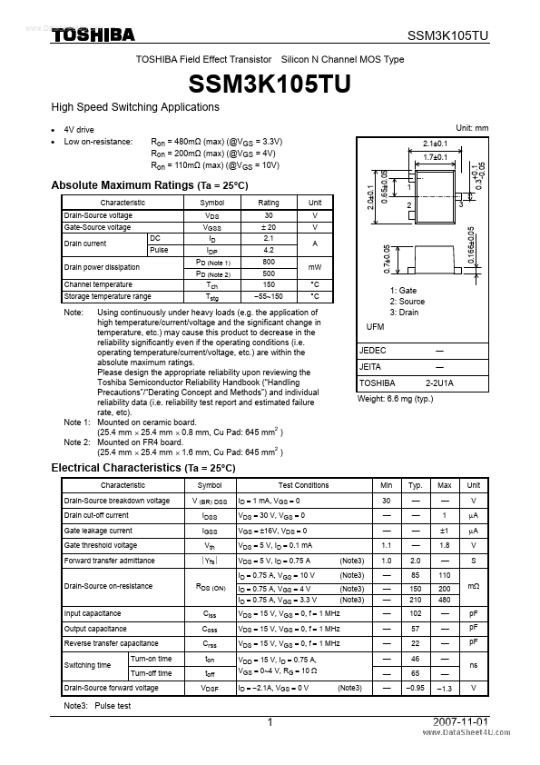
- - 4V drive Low on-resistance: Unit: mm Ron = 480mΩ (max) (@VGS = 3.3V) Ron = 200mΩ (max) (@VGS = 4V) Ron = 110mΩ (max) (@VGS = 10V)
2.0±0.1 2.1±0.1 1.7±0.1 0.65±0.05 +0.1 0.3 -0.05 3 0.166±0.05
Absolute Maximum Ratings (Ta = 25°C)
Characteristic Drain-Source voltage Gate-Source voltage Drain current Drain power dissipation Channel temperature Storage temperature range DC Pulse Symbol VDS VGSS ID IDP PD (Note 1) PD (Note 2) Tch Tstg Rating 30 ± 20 2.1 4.2 800 500 150
- 55~150 Unit V V
1 2 m W °C °C
Using continuously under heavy loads (e.g. the application of high temperature/current/voltage and the significant change in temperature, etc.) may cause this product to decrease in the reliability significantly even if the operating conditions (i.e. operating temperature/current/voltage, etc.) are within the absolute maximum ratings. Please design the appropriate reliability upon reviewing the Toshiba Semiconductor Reliability Handbook (“Handling Precautions”/“Derating Concept and Methods”) and individual reliability data (i.e. reliability test report and estimated failure rate, etc). Note 1: Mounted on ceramic board. 2 (25.4 mm × 25.4 mm × 0.8 mm, Cu Pad: 645 mm ) Note 2: Mounted on FR4 board. (25.4 mm × 25.4 mm × 1.6 mm, Cu Pad: 645 mm2 )
Note:
UFM JEDEC JEITA TOSHIBA ― ― 2-2U1A
Weight: 6.6 mg (typ.)
Electrical Characteristics (Ta = 25°C)
Characteristic Drain-Source breakdown voltage Drain cut-off current Gate leakage current Gate threshold voltage Forward transfer admittance Symbol V (BR) DSS IDSS IGSS Vth ⏐Yfs⏐ RDS (ON) Ciss Coss Crss ton toff VDSF Test Conditions ID = 1 m A, VGS = 0 VDS = 30 V, VGS = 0 VGS = ±16V, VDS = 0 VDS = 5 V, ID = 0.1 m A VDS = 5 V, ID = 0.75 A ID = 0.75 A, VGS = 10 V Drain-Source on-resistance ID = 0.75 A, VGS = 4 V ID = 0.75 A, VGS = 3.3 V Input capacitance Output capacitance Reverse transfer capacitance Switching...