Datasheet4U Logo Datasheet4U.com
Toshiba logo

TCK402G

Manufacturer: Toshiba

TCK402G datasheet by Toshiba.

This datasheet includes multiple variants, all published together in a single manufacturer document.

TCK402G datasheet preview

TCK402G Datasheet Details

Part number TCK402G
Datasheet TCK402G TCK401G Datasheet (PDF)
File Size 499.27 KB
Manufacturer Toshiba
Description External FET Driver IC
TCK402G page 2 TCK402G page 3

TCK402G Overview

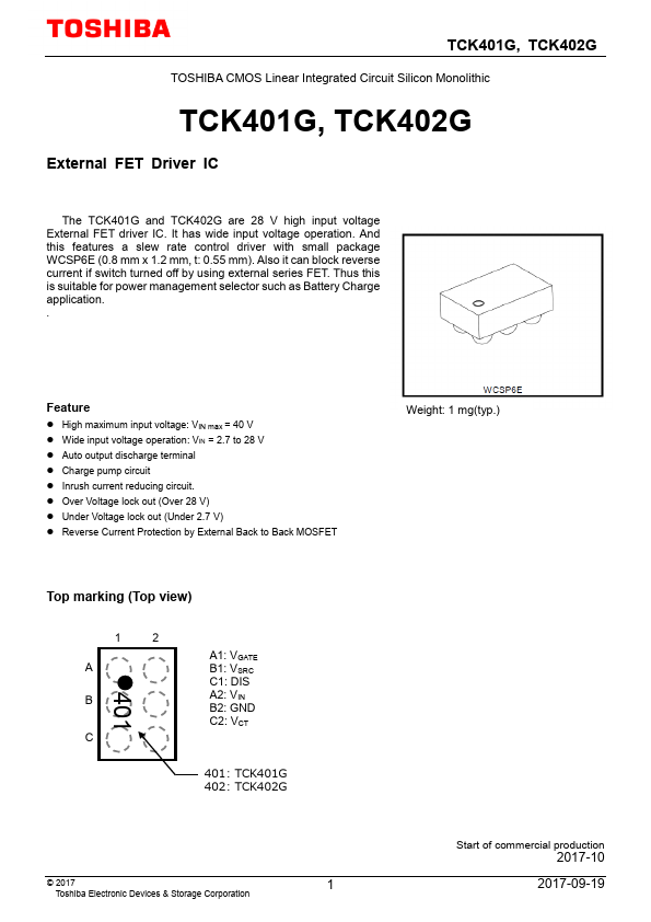
TCK401G, TCK402G TOSHIBA CMOS Linear Integrated Circuit Silicon Monolithic TCK401G, TCK402G External FET Driver IC The TCK401G and TCK402G are 28 V high input voltage External FET driver IC. It has wide input voltage operation.

TCK402G Key Features

  • High maximum input voltage: VIN max = 40 V
  • Wide input voltage operation: VIN = 2.7 to 28 V
  • Auto output discharge terminal
  • Charge pump circuit
  • Inrush current reducing circuit
  • Over Voltage lock out (Over 28 V)
  • Under Voltage lock out (Under 2.7 V)
  • Reverse Current Protection by External Back to Back MOSFET
Toshiba logo - Manufacturer

More Datasheets from Toshiba

View all Toshiba datasheets

Part Number Description
TCK401G External FET Driver IC
TCK101G 1A Load Switch
TCK1024G Load Switch
TCK102G 1A Load Switch
TCK104G Load Switch
TCK105G Load Switch
TCK106AG 1.0A Load Switch
TCK107AG 1.0A Load Switch
TCK108AG 1.0A Load Switch
TCK111G Ultra Low On resistance Load Switch

TCK402G Distributor

Datasheet4U Logo
Since 2006. D4U Semicon. About Datasheet4U Contact Us Privacy Policy Purchase of parts