TCK401G Overview
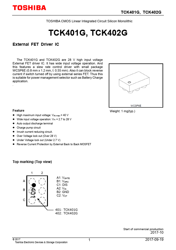
TCK401G, TCK402G TOSHIBA CMOS Linear Integrated Circuit Silicon Monolithic TCK401G, TCK402G External FET Driver IC The TCK401G and TCK402G are 28 V high input voltage External FET driver IC. It has wide input voltage operation.
TCK401G Key Features
- High maximum input voltage: VIN max = 40 V
- Wide input voltage operation: VIN = 2.7 to 28 V
- Auto output discharge terminal
- Charge pump circuit
- Inrush current reducing circuit
- Over Voltage lock out (Over 28 V)
- Under Voltage lock out (Under 2.7 V)
- Reverse Current Protection by External Back to Back MOSFET