TC7WPB8306L8X Overview
Key Features
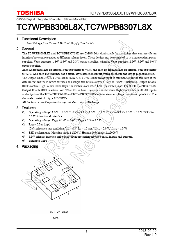
- Packaging MP8 1 2013-02-20 Rev.1.0
- Pin Assignment TC7WPB8306L8X TC7WPB8306L8X,TC
| Part | TC7WPB8306L8X |
|---|---|
| Description | 2-Bit Dual-Supply Bus Switch |
| Manufacturer | Toshiba |
| Size | 240.89 KB |
| Part Number | Manufacturer | Description |
|---|---|---|
| SW-331 | Tyco Electronics | Matched GaAs SPDT Switch |
| B3045G | onsemi | Switch-mode Power Rectifiers |
| DK1203 | Dongke Semiconductor | AC-DC Switch Mode Power controller |