Datasheet4U.com
🌙
TC7USB3212WBG Datasheet | Toshiba
Part:
TC7USB3212WBG
Description:
Quad SPDT USB Switch
Manufacturer:
Toshiba
Size:
245.49 KB
TC7USB3212WBG Datasheet (PDF) Download
Toshiba
TC7USB3212WBG
Key Features
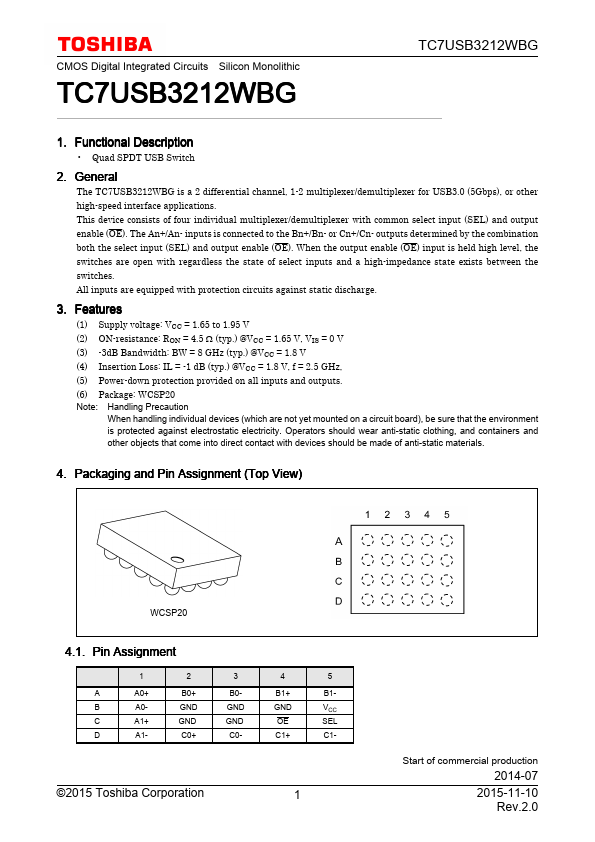
Packaging and Pin Assignment (Top View) WCSP20
×
Close