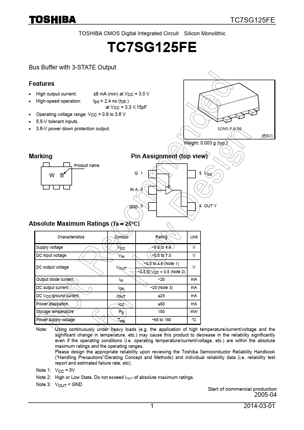
Datasheet4U Logo Datasheet4U.com

TC7SG125FE - Bus Buffer

Features

  • High output current: ±8 mA (min) at VCC = 3.0 V.
  • High-speed operation: tpd = 2.4 ns (typ. ) at VCC = 3.3 V,15pF.
  • Operating voltage range: VCC = 0.9 to 3.6 V.
  • 5.5-V tolerant inputs.
  • 3.6-V power down protection output. Marking WB Product name Weight: 0.003 g (typ. ) Pin Assignment (top view) G1 5 VCC IN A 2 (ESV) GND 3 4 OUT Y Absolute Maximum Ratings (Ta = 25°C) Characteristics Symbol Rating Unit Supply voltage DC input voltage DC.

📥 Download Datasheet

Full PDF Text Transcription (Reference)

The following content is an automatically extracted verbatim text from the original manufacturer datasheet and is provided for reference purposes only.

View original datasheet text
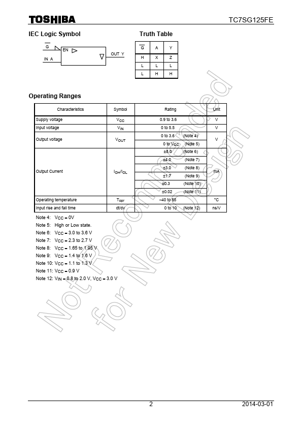
TC7SG125FE TOSHIBA CMOS Digital Integrated Circuit Silicon Monolithic TC7SG125FE Bus Buffer with 3-STATE Output Features • High output current: ±8 mA (min) at VCC = 3.0 V • High-speed operation: tpd = 2.4 ns (typ.) at VCC = 3.3 V,15pF • Operating voltage range: VCC = 0.9 to 3.6 V • 5.5-V tolerant inputs. • 3.6-V power down protection output. Marking WB Product name Weight: 0.003 g (typ.) Pin Assignment (top view) G1 5 VCC IN A 2 (ESV) GND 3 4 OUT Y Absolute Maximum Ratings (Ta = 25°C) Characteristics Symbol Rating Unit Supply voltage DC input voltage DC output voltage Output diode current DC output current DC VCC/ground current Power dissipation Storage temperature Power supply voltage VCC VIN VOUT IIK IOK IOUT ICC PD Tstg −0.5 to 4.6 V −0.5 to 7.0 V −0.
Published: |