Datasheet4U Logo Datasheet4U.com

TC7QPB9307FK - Low Voltage / Low Power 4-Bit Dual Supply Bus Switch

Download the TC7QPB9307FK datasheet PDF. This datasheet also covers the TC7QPB9306FK variant, as both devices belong to the same low voltage / low power 4-bit dual supply bus switch family and are provided as variant models within a single manufacturer datasheet.

Key Features

  • Operating voltage:1.8 V to 2.5 V, 1.8 V to 3.3 V, 1.8 V to 5.0 V, 2.5 V to 3.3 V, 2.5 V to 5.0 V, 3.3 V to 5.0 V bidirectional interface.
  • Operating voltage: VCCA = 1.65 to 5.0 V, VCCB = 2.3 to 5.5 V.
  • Low ON-resistance: RON = 5.0 Ω (typ. ) @ VIS = 0 V, IIS = 30 mA, VCCA= 3.0 V, VCCB = 4.5 V.
  • ESD performance: Machine model ≥ ±200 V Human body model ≥ ±2000 V.
  • 5.5 V tolerance and power-down protection at the Output Enable input.
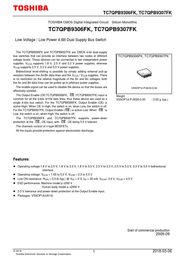
  • Packages: VSSOP14(US14) © 2018 1 Tos.

📥 Download Datasheet

Note: The manufacturer provides a single datasheet file (TC7QPB9306FK-Toshiba.pdf) that lists specifications for multiple related part numbers.

Datasheet Details

Part number TC7QPB9307FK
Manufacturer Toshiba
File Size 562.60 KB
Description Low Voltage / Low Power 4-Bit Dual Supply Bus Switch
Datasheet download datasheet TC7QPB9307FK Datasheet

Full PDF Text Transcription (Reference)

The following content is an automatically extracted verbatim text from the original manufacturer datasheet and is provided for reference purposes only.

View original datasheet text
TC7QPB9306FK, TC7QPB9307FK TOSHIBA CMOS Digital Integrated Circuit Silicon Monolithic TC7QPB9306FK, TC7QPB9307FK Low Voltage / Low Power 4-Bit Dual Supply Bus Switch The TC7QPB9306FK and TC7QPB9307FK are CMOS 4-bit dual-supply bus switches that can provide an interface between two nodes at different voltage levels. These devices can be connected to two independent power supplies. VCCA supports 1.8 V, 2.5 V and 3.3 V power supplies, whereas VCCB supports 2.5 V, 3.3 V and 5.0 V power supplies. Bidirectional level-shifting is possible by simply adding external pull-up resistors between the An/Bn data lines and the VCCA / VCCB supplies. There is no restriction on the relative magnitude of the An and Bn voltages; both the An and Bn data lines can be pulled up to arbitrary power supplies.