Datasheet4U Logo Datasheet4U.com

TC7PB53TU - Single 1-of-2 Demultiplexer

Key Features

  • Operating voltage range : VCC = 2 to 3.6 V.
  • High-speed operation : tpd = 50 ns (max) @ 2.7 V.
  • Very low ON-resistance : RON = 3Ω (max) @ 2.7 V.
  • High latch-up immunity : ±300 mA.
  • ESD performance : Machine model ≥ ±200 V Human body model ≥ ±2000 V.
  • Package : UF6 Pin Assignment (top view) Ch1 1 GND 2 6A 5 VCC Marking EBB Product name Ch0 3 4 COM Start of commercial production 2004-05 1 2014-03-01 Truth Table Input A L H Funct.

📥 Download Datasheet

Datasheet Details

Part number TC7PB53TU
Manufacturer Toshiba
File Size 195.29 KB
Description Single 1-of-2 Demultiplexer
Datasheet download datasheet TC7PB53TU Datasheet

Full PDF Text Transcription (Reference)

The following content is an automatically extracted verbatim text from the original manufacturer datasheet and is provided for reference purposes only.

View original datasheet text
TC7PB53TU TOSHIBA CMOS Digital Integrated Circuit Silicon Monolithic TC7PB53TU 
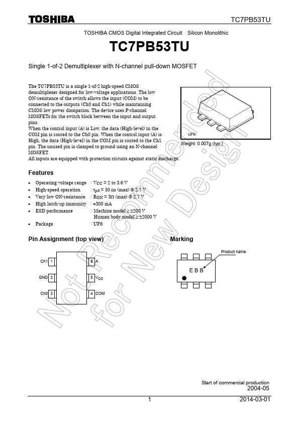
Single 1-of-2 Demultiplexer with N-channel pull-down MOSFET The TC7PB53TU is a single 1-of-2 high-speed CMOS demultiplexer designed for low-voltage applications. The low ON-resistance of the switch allows the input (COM) to be connected to the outputs (Ch0 and Ch1) while maintaining CMOS low power dissipation. The device uses P-channel MOSFETs for the switch block between the input and output pins. When the control input (A) is Low, the data (High-level) in the COM pin is routed to the Ch0 pin. When the control input (A) is High, the data (High-level) in the COM pin is routed to the Ch1 pin. The unused pin is clamped to ground using an N-channel Weight: 0.007g (typ.) MOSFET.