TC74VHC125FK
TC74VHC125FK is Quad Bus Buffer manufactured by Toshiba.
- Part of the TC74VHC125 comparator family.
- Part of the TC74VHC125 comparator family.
TC74VHC125,126F/FK
TOSHIBA CMOS Digital Integrated Circuit Silicon Monolithic
TC74VHC125F, TC74VHC125FK TC74VHC126F, TC74VHC126FK
TC74VHC125F/FK TC74VHC126F/FK
Quad Bus Buffer Quad Bus Buffer
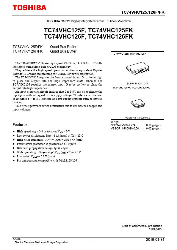
TC74VHC125F, TC74VHC126F
The TC74VHC125/126 are high speed CMOS QUAD BUS BUFFERs fabricated with silicon gate C2MOS technology.
They achieve the high speed operation similar to equivalent Bipolar Shottky TTL while maintaining the CMOS low power dissipation.
The TC74VHC125 requires the 3-state control input G to be set high to place the output into the high impedance state, whereas the TC74VHC126 requires the control input G to be set low to place the output into high impedance.
An input...