Datasheet4U Logo Datasheet4U.com

TC74VCX74FK - Low-Voltage Dual D-Type Flip-Flop

Download the TC74VCX74FK datasheet PDF (TC74VCX74FT included). The manufacturer datasheet provides complete specifications, pinout details, electrical characteristics, and typical applications for low-voltage dual d-type flip-flop.

Features

  • Low-voltage operation: VCC = 1.2 to 3.6 V.
  • High-speed operation: tpd = 3.5 ns (max) (VCC = 3.0 to 3.6 V) : tpd = 4.6 ns (max) (VCC = 2.3 to 2.7 V) : tpd = 9.2 ns (max) (VCC = 1.65 to 1.95 V) : tpd = 18.4 ns (max) (VCC = 1.4 to 1.6 V) : tpd = 46.0ns (max) (VCC = 1.2 V).
  • Output current: IOH/IOL = ±24 mA (min) (VCC = 3.0 V) : IOH/IOL = ±18 mA (min) (VCC = 2.3 V) : IOH/IOL = ±6 mA (min) (VCC = 1.65 V) : IOH/IOL = ±2 mA (min) (VCC = 1.4 V).
  • Latch-up performance:.

📥 Download Datasheet

Note: The manufacturer provides a single datasheet file (TC74VCX74FT_ToshibaSemiconductor.pdf) that lists specifications for multiple related part numbers.
Other Datasheets by Toshiba

Full PDF Text Transcription

Click to expand full text
TC74VCX74FT/FK TOSHIBA CMOS Digital Integrated Circuit Silicon Monolithic 
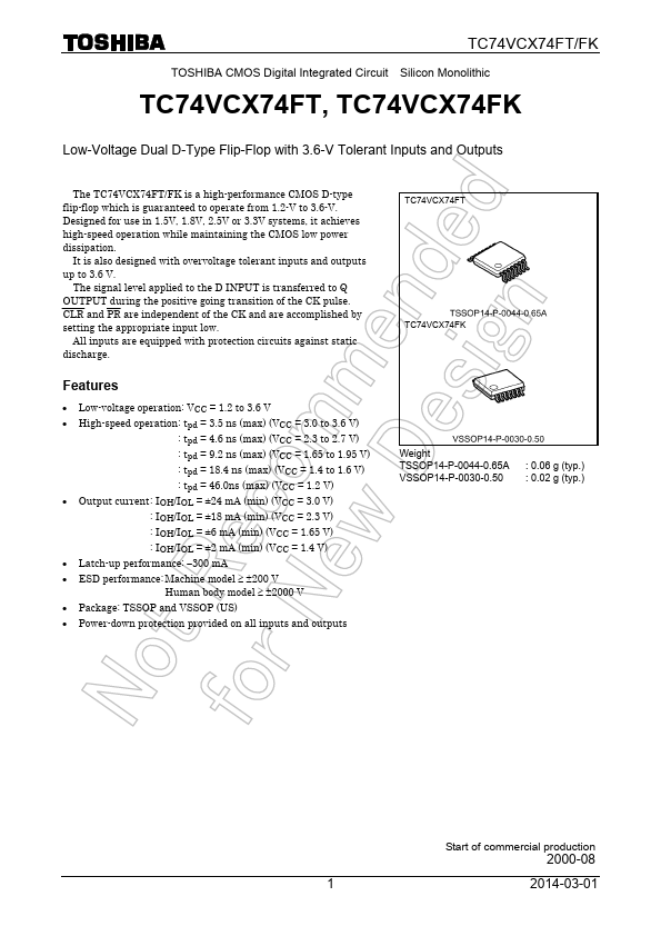
TC74VCX74FT, TC74VCX74FK Low-Voltage Dual D-Type Flip-Flop with 3.6-V Tolerant Inputs and Outputs The TC74VCX74FT/FK is a high-performance CMOS D-type flip-flop which is guaranteed to operate from 1.2-V to 3.6-V. Designed for use in 1.5V, 1.8V, 2.5V or 3.3V systems, it achieves high-speed operation while maintaining the CMOS low power dissipation. It is also designed with overvoltage tolerant inputs and outputs up to 3.6 V. 
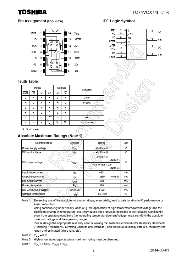
The signal level applied to the D INPUT is transferred to Q OUTPUT during the positive going transition of the CK pulse. CLR and PR are independent of the CK and are accomplished by setting the appropriate input low. All inputs are equipped with protection circuits against static discharge.
Published: |